NINA-W1 series - System integration manual
UBX-17005730 - R11 Handling and soldering Page 45 of 55
C1 - Public
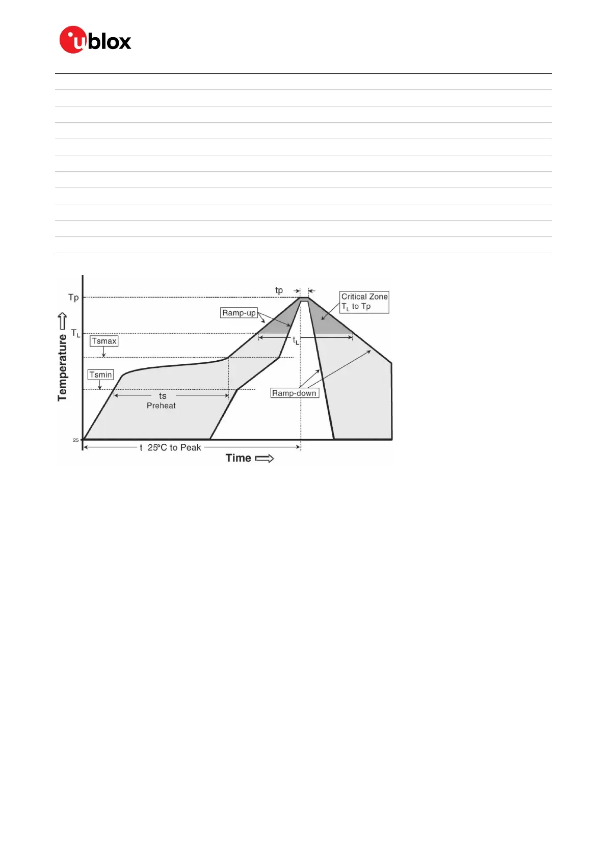
Process parameter Unit Value
Pre-heat Ramp up rate to T
SMIN
K/s 3
T
SMIN
°C 150
T
SMAX
°C 200
t
S
(from +25 °C) s 150
t
S
(Pre-heat) s 60 to 120
Peak T
L
°C 217
t
L
(time above T
L
) s 40 to 60
T
P
(absolute max) °C 245
Cooling Ramp-down from T
L
K/s 4
Allowed soldering cycles - 1
Table 6: Recommended reflow profile
Figure 30: Reflow profile
Lower value of T
P
and slower ramp down rate (2 – 3 °C/sec) is preferred.
After reflow soldering, optical inspection of the modules is recommended to verify proper alignment.
⚠ The target values given in Table 6 should be regarded as general guidelines for a Pb-free process.
Refer to JEDEC J-STD-020C standard for further information.
4.3.2 Cleaning
Cleaning the modules is not recommended. Residues underneath the modules cannot be easily
removed with a washing process.
• Cleaning with water will lead to capillary effects where water is absorbed in the gap between the
baseboard and the module. The combination of residues of soldering flux and encapsulated water
leads to short circuits or resistor-like interconnections between neighboring pads. Water will also
damage the sticker and the ink-jet printed text.
• Cleaning with alcohol or other organic solvents can result in soldering flux residues flooding into
the two housings, areas that are not accessible for post-wash inspections. The solvent will also
damage the sticker and the ink-jet printed text.
• Ultrasonic cleaning will permanently damage the module, in particular the crystal oscillators.
For best results, use a "no clean" soldering paste and eliminate the cleaning step after the soldering
process.
 Loading...