13.
With
FREQ
DIAL
still fully clockwise,
set the voltage 26. Adjust R165
for
a 2.5
V
p-p
signal
output
from
the
between IC2(2)
and
ground (at R95) to 0
Vdc sine amplifier
±25 mV.
±100
/iV,
using
R93.
14.
Set
FREQ DIAL to
1
and adjust
voltage between
TP6 and TP7 to
0
Vdc ±200
juV, using R129.
15. Adjust
voltage
between TPS and
TP9
to 0
Vdc
±200
juV, using
R 1 32.
4.2.5
Triangle Amplitude
Adjustment
16.
Set
FREQ HZ to
X
100,
FREQ
DIAL to
10,
WAVE-
FQRM SELECTOR to
TRIANGLE,
and
SYMMETRY
to
NORM.
17.
Connect the
oscilloscope probe (a
type W or 1A5
plug-in module
should be used
with the scope) to
\
position
of the
WAVEFORM selector
switch,
SW2,
see
Figure
4-4.
18.
Adjust
the triangle
amplitude to
±1.25 V
±5 mV,
using
R12 and R23,
see
Drawing
142-010.
4.2.6
Sine
Distortion
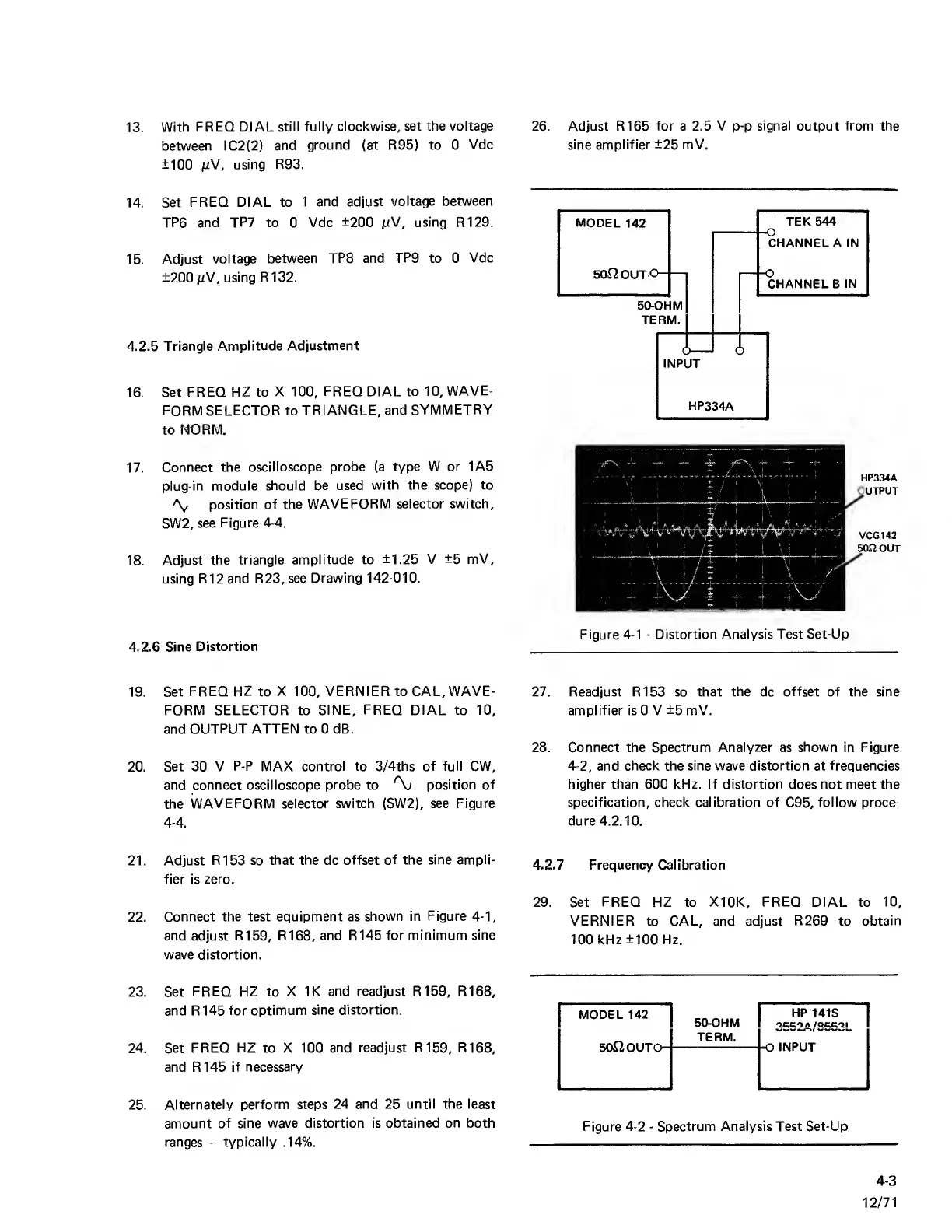
Figure
4-1
-
Distortion Analysis Test
Set-Up
19. Set
FREQ HZ
to
X
100,
VERNIER to CAL, WAVE-
FORM SELECTOR to
SINE,
FREQ
DIAL to
10,
and
OUTPUT ATTEN to 0 dB.
20.
Set 30 V
P-P
MAX
control to 3/4ths of full
CW,
and connect oscilloscope
probe
to
position of
the
WAVEFORM selector switch (SW2), see Figure
4-4.
27. Readjust R153 so that
the
dc
offset
of the sine
amplifier
is 0 V
±5
mV.
28. Connect the Spectrum
Analyzer
as
shown
in Figure
4-2, and
check the sine wave distortion at frequencies
higher than
600
kHz. If distortion
does
not
meet
the
specification, check calibration of
C95,
follow proce-
dure 4.2.10.
21. Adjust
R153 so
that the
dc
offset of the sine ampli-
fier is
zero.
22.
Connect the test equipment as
shown in
Figure
4-1,
and
adjust
R159, R168, and
R145 for
minimum sine
wave distortion.
23. Set
FREQ HZ to X
IK and readjust R159, R168,
and R145
for optimum
sine distortion.
24. Set
FREQ HZ to X 100
and readjust R159, R168,
and R145
if necessary
25. Alternately
perform steps
24 and 25 until the least
amount
of sine wave distortion is obtained
on
both
ranges
—
typically
.14%.
4.2.7
Frequency Calibration
29.
Set
FREQ
HZ to
X10K, FREQ
DIAL to
10,
VERNIER to
CAL, and
adjust
R269
to
obtain
100 kHz ±100 Hz.
MODEL 142
HP
141S
50-OHM
TERM.
50J2OUTO-
-O
INPUT
Figure
4-2
-
Spectrum Analysis Test Set-Up
4-3
12/71