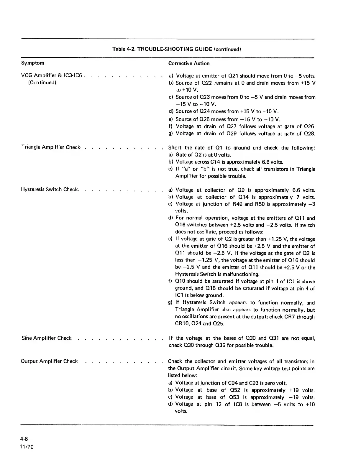
Table
4-2.
TROUBLE-SHOOTING
GUIDE
(continued)
Symptom
Corrective
Action
VCG Amplifier
&
IC3-IC6
.
a) Voltage at emitter of Q21 should
move
from
0 to
—5
volts.
(Continued)
b) Source of Q22
remains at 0 and drain moves from
+15
V
to+IOV.
c) Source of Q23 moves from
0 to
—5
V
and drain moves from
-15
V
to -10
V.
d)
Source of Q24
moves from +15 V
to
+10 V,
e) Source of Q25 moves from
—15
V
to
—10
V.
f)
Voltage
at drain of
Q27 follows voltage at gate of Q26.
g)
Voltage
at
drain
of
Q29 follows voltage
at gate of Q28.
Triangle
Amplifier
Check-
Short
the gate of Q1 to ground and check
the following:
a) Gate
of Q2 is
at 0
volts.
b) Voltage across
C14
is approximately
6.6 volts.
c)
If
"a" or "b" is not true, check all
transistors in Triangle
Amplifier for
possible trouble.
Hysteresis Switch Check
a) Voltage
at collector of
Q9 is approximately
6.6
volts.
b) Voltage
at collector of
Q14 is approximately
7 volts.
c) Voltage
at
junction of R49
and R50 is approximately
—3
volts.
d)
For
normal operation,
voltage
at
the emitters
of Q1
1 and
Q16 switches
between +2.5
volts and
—2.5
volts. If switch
does
not oscillate, proceed
as
follows:
e)
If
voltage
at gate of
Q2 is greater than +1.25
V, the voltage
at the
emitter
of
Q16 should
be +2.5 V and the
emitter
of
Q1 1 should
be
—2.5
V. If
the voltage at the gate of Q2 is
less
than
—1.25
V,
the voltage
at the emitter
of
Q16
should
be
—2.5
V
and the
emitter of
Q1
1
should
be +2.5
V or the
Hysteresis
Switch is
malfunctioning.
f)
Q10 should
be saturated if voltage
at
pin
1
of
IC1 is
above
ground,
and
Q15 should
be saturated if voltage
at pin 4 of
IC1
is below ground.
g)
If
Hysteresis
Switch appears
to function
normally,
and
Triangle
Amplifier
also appears
to function normally,
but
no oscillations
are
present at the
output; check CR7 through
CR10, Q24
and Q25.
Sine Amplifier Check
If
the voltage at the bases of Q30 and Q31 are not equal,
check Q30 through
Q35 for possible trouble.
Output Amplifier Check Check the collector
and emitter
voltages
of
all transistors
in
the
Output Amplifier circuit.
Some key voltage test points are
listed below:
a) Voltage
at junction
of
C94 and
C93
is zero volt.
b)
Voltage
at
base of Q52 is
approximately +19 volts.
c) Voltage
at
base of
Q53 is approximately
—19
volts.
d) Voltage
at pin
12 of
ICS is between
-5
volts
to
+10
volts.
4-6
11/70