Do you have a question about the Xilinx Spartan-6 LX9 and is the answer not in the manual?
Explains the purpose of the manual and the contents of the Avnet Spartan-6 FPGA LX9 MicroBoard kit.
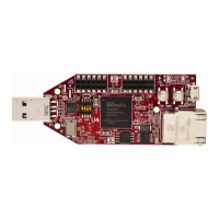
Lists the main hardware components and features of the Spartan-6 FPGA LX9 MicroBoard.
Details where to find reference designs demonstrating potential applications of the MicroBoard.
Lists the evaluation kit part numbers and available software options for purchase.
Details the Xilinx XC6SLX9-2CSG324C FPGA, its family, technology, and features.
Describes the CDCE913 clock synthesizer and optional oscillator, including frequencies.
Details the LPDDR SDRAM and SPI Flash memory components used on the board.
Describes the Micron LPDDR Mobile SDRAM, its architecture, and interface.
Details the 128 Mb Micron SPI Flash memory for configuration and data storage.
Describes USB-to-JTAG, USB-to-UART, and 10/100 Ethernet communication ports.
Details the PMOD connectors for interfacing with external modules.
Describes user LEDs, DIP switches, and push-buttons for user interaction.
Explains the power circuitry, voltage regulators, and power sequencing.
Outlines the three methods for configuring the FPGA on the MicroBoard.
Describes the factory test programmed into the SPI Flash and how to access test source code.
Lists key partners and their contributions to the Spartan-6 FPGA LX9 MicroBoard project.
Provides information on accessing Avnet and Xilinx technical support and online resources.
Details the changes made in each revision of the MicroBoard User Guide.
| Logic Cells | 9152 |
|---|---|
| Registers | 11440 |
| Slices | 1430 |
| Block RAM (Kb) | 576 |
| DSP48A1 Slices | 16 |
| Number of I/O Banks | 4 |
| Input Delay Blocks | Yes |
| Output Delay Blocks | Yes |
| Maximum Single-Ended Output Current (mA) | 24 |
| I/O Standards Supported | LVTTL, LVCMOS, PCI, SSTL, HSTL |
| Maximum Differential Output Current (mA) | 12 |