Copyright © 2015 Avnet, Inc. AVNET and the AV logo are registered trademarks of Avnet, Inc. All other brands are property of their respective owners.
Avnet Electronics Marketing 6 of 28 Rev D 24 Apr 2015
1.3 Reference Designs
Reference designs that demonstrate some of the potential applications of the Spartan-6 FPGA LX9 MicroBoard
are available and can be found on the Avnet Electronics Marketing Design Resource Center (DRC) web site:
www.em.avnet.com/s6microboard. See the PDF document included with each reference design for a complete
description of the design and detailed instructions for running a demonstration on the development board.
Check the DRC periodically for updates and new designs. The Expanded Getting Started Guide, available for
download from the DRC, is the best place to start.
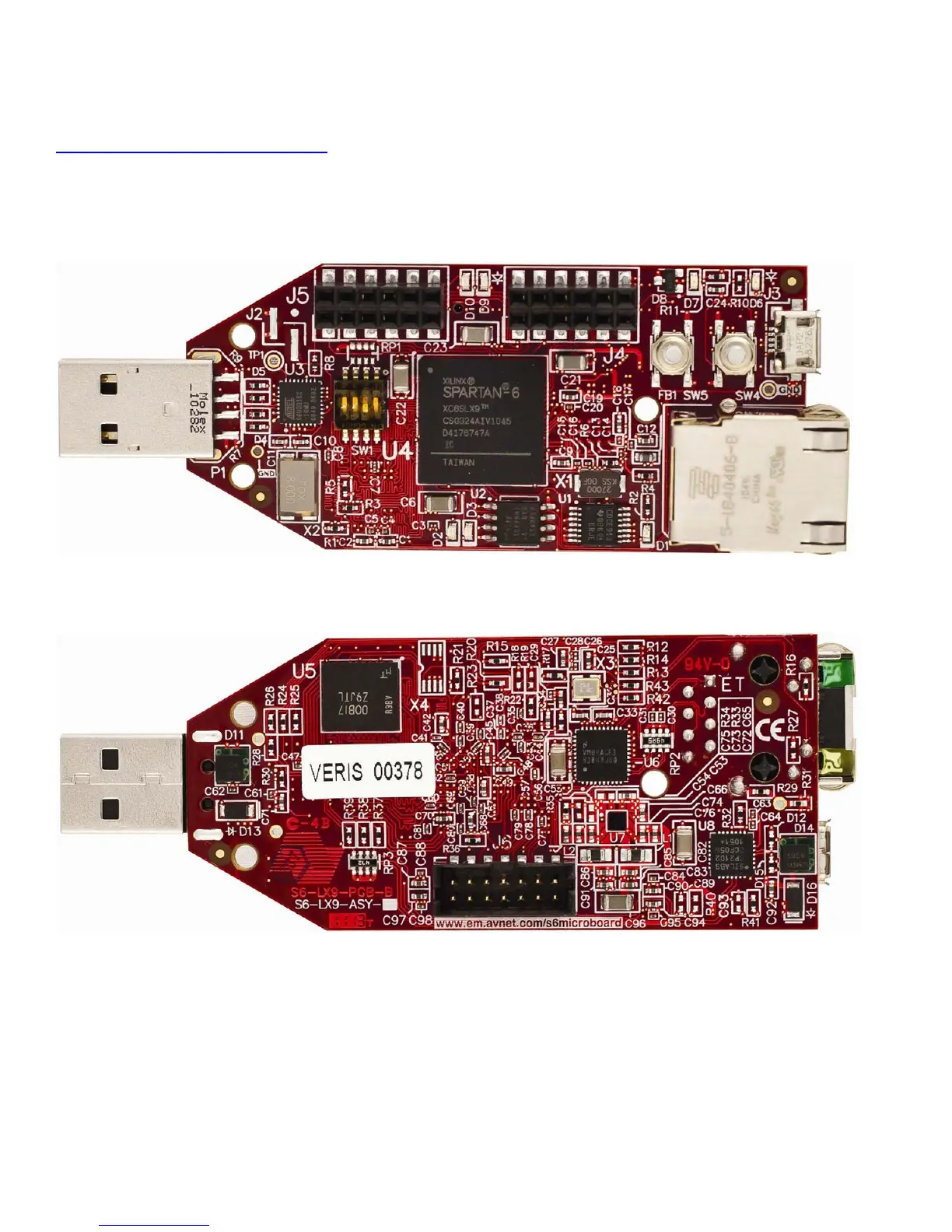
Figure 1 – Spartan-6 FPGA LX9 MicroBoard Front
Figure 2 – Spartan-6 FPGA LX9 MicroBoard Back
 Loading...