Copyright © 2015 Avnet, Inc. AVNET and the AV logo are registered trademarks of Avnet, Inc. All other brands are property of their respective owners.
Avnet Electronics Marketing 8 of 28 Rev D 24 Apr 2015
2 Functional Description
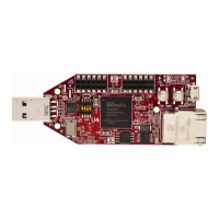
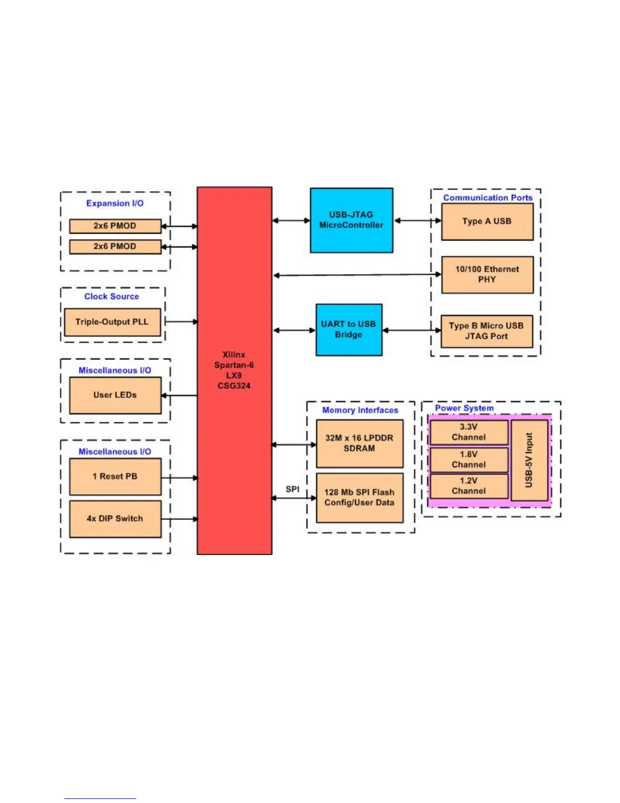
A Xilinx Spartan-6 FPGA LX9 (XC6SLX9-2CSG324) FPGA is the primary component of the Avnet Spartan-6
FPGA LX9 MicroBoard. A 10/100 Ethernet port and two Full Speed USB interfaces provide means of off-
board communication. On-board memory consists of a 256 Mbit x 16 LPDDR mobile SDRAM component and
a 128 Mbit Multi-I/O SPI Flash that may be used by the FPGA for configuration.
A high-level block diagram of the Spartan-6 FPGA LX9 MicroBoard is shown below followed by a brief
description of each sub-section.
Figure 3 – Spartan-6 FPGA LX9 MicroBoard Block Diagram
 Loading...