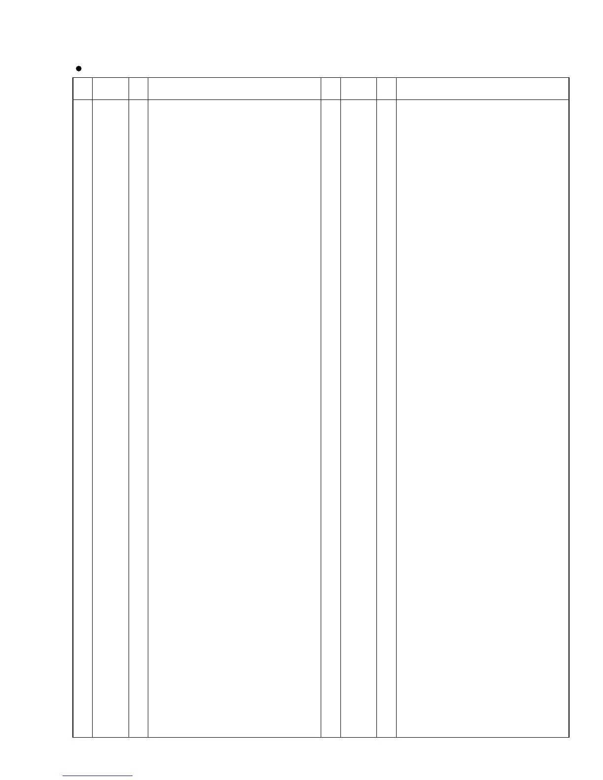
23
O1X
PIN
NO.
I/O FUNCTIONNAME
PIN
NO.
I/O FUNCTIONNAME
mLAN-NC1 (X2150A00) mLAN
TM
Node Controller 1
1 VDD Power terminal
2 TEST5 I Test terminal
3 TEST4 I Test terminal
4 TEST3 I Test terminal
5 TEST2 I Test terminal
6 TEST1 I Test terminal
7 SCANE I Test terminal
8 TRST I JTAG terminal
9 TMS I JTAG terminal
10 TCK I JTAG terminal
11 VSS Ground terminal
12 TDO O JTAG terminal
13 TDI I JTAG terminal
14 SCL O EEPROM serial clock
15 SDA I/O EEPROM serial data
16
ASYNCFLG
I/O Asynchronous flag
17 ISOFLG I/O Isochronous flag
18 BUSRST O Bus reset
19 VDD Power terminal
20 D7 I/O PHY I/F data bus
21 D6 I/O PHY I/F data bus
22 D5 I/O PHY I/F data bus
23 D4 I/O PHY I/F data bus
24 VSS Ground terminal
25 D3 I/O PHY I/F data bus
26 D2 I/O PHY I/F data bus
27 D1 I/O PHY I/F data bus
28 D0 I/O PHY I/F data bus
29 VDD Power terminal
30 CTL1 I/O PHY-LINK control: Control signal for interface
with PHY chip
31 CTL0 I/O PHY-LINK control: Control signal for interface
with PHY chip
32 VSS Ground terminal
33 SCLK I Master clock
34 VDD Power terminal
35 LREQ O Link request
36 VSS Ground terminal
37 LPS O Link power status
38 DAI0 I Digital audio input 0 /MIDI input 4
39 DAI1 I Digital audio input 1 /MIDI input 5
40 DAI2 I Digital audio input 2 /MIDI input 6
41 DAI3 I Digital audio input 3 /MIDI input 7
42 BCKI I Bit clock input for digital audio input
43 WCKI I Word clock input for digital audio input
44 DITI I
Audio data input when using built-in DIT separately
45 DIT MCI I Master clock input when using built-in DIT
separately (128Fs clock)
46 DIT BCI I Bit clock input when using built-in DIT
separately (32Fs to 128Fs)
47 DIT WCI I Word clock input when using built-in DIT
separately
48 SLV I Master: L, Slave : H when using a multiple
number of packet handler chips simultaneously,
fixed at Low when using mLAN-NC1 only
49 SEQI I Loop connection input pin when using a multiple
number of packet handler chips simultaneously,
fixed at Low when using mLAN-NC1 only
50 VSS Ground terminal
51 ECKI I
Bit clock input for reception from outside (128Fs clock)
52 EWCKI I Word clock input for reception from outside
53 EWCKI2 I Word clock input for PSC4
54 ECKI2 I Bit clock input for PSC4 (128Fs clock)
55 SEQO O Loop connection output pin when using a
multiple number of packet handler chips
simultaneously
56 ECKO O Bit clock output for reception to outside (128Fx)
57 EWCKO O Word clock output for reception to outside
58 DAO0 O Digital audio output 0/MIDI output 4
59 VDD Power terminal
60 DAO1 O Digital audio output 1/MIDI output 5
61 DAO2 O Digital audio output 2/MIDI output 6
62 DAO3 O Digital audio output 3/MIDI output 7
63 BCKO O
Bit clock output for digital audio output (64Fs clock)
64 VSS Ground terminal
65 WCKO O Word clock output for digital audio output
66 MCKO O Master clock output for digital audio output
67 WCKOD O Delay output of WCKO
68 IEC958O O IEC60958 signal output from built-in DIT
69
INT R SEL
I Selection of PLL division rate setting bit for SYT
70
SEL MCK1
I MCKO division rate setting bit 1
71
SEL MCK0
I MCKO division rate setting bit 0
72
SEL VCO1
I PLL division rate setting bit 1 for SYT
73
SEL VCO0
I PLL division rate setting bit 0 for SYT
74 AUX1 I PLL external VCO clock input for SYT
75 VDD Power terminal
76 PCA O PLL external phase comparator output for SYT
77 PCB O PLL external phase comparator output for SYT
78 LOCKN1 O PLL lock flag output for SYT
79 VSS Ground terminal
80
VCO 01 CLK
I External VCXO input for digital PLL1 (SYT)
81 VDD Power terminal
82
PLL 01 Pump SK
TRI Pump signal to sink current for PLL1
83 VSS Ground terminal
84
PLL 01 Pump SC
TRI Pump signal to source current for PLL1
85 VDD Power supply terminal
86
VCO 02 CLK
I External VCO input for digital PLL2 (SYT)
87 VSS Ground terminal
88
PLL 02 Pump SK
TRI Pump signal to sink current for PLL2
89 VDD Power terminal
90
PLL 02 Pump SC
TRI Pump signal to source current for PLL2
91 VSS Ground terminal
92 MI0 I MIDI input 0
93 MI1 I MIDI input 1
94 MI2 I MIDI input 2
95 MI3 I MIDI input 3
96 VDD Power supply terminal
97 MO0 O MIDI output 0
98 MO1 O MIDI output 1
99 MO2 O MIDI output 2
100 MO3 O MIDI output 3
101 VSS Ground terminal
102 DIR SCK O To SCK of DIR5
103 DIR SO O To SI of DIR5
104 DIR SI I(PU) To SO of DIR5
105 DIR CSN O To /CS of DIR5
106 DIR INT I To INT of DIR5
107
DIR LOCKN
I To /LOCK of DIR5
108 ERR BS I To ERR/BS of DIR5
109 VDD Power terminal
110
XTAL(OSC3)
I MPU clock oscillation circuit terminal
111
XTAL(OSC4)
O MPU clock oscillation circuit output terminal
112 VSS Ground terminal
113 DBL V I To DBL/V of DIR5
114 FS128 C I To FS128/C of DIR5
115 SYNC U I To SYNC/U of DIR5
116 DIR SDI I To SDO of DIR5
117 VDD Power terminal
118 WRH# I/O Write enable high: host data bus
119 WAIT# I/O External bus wait signal
120 WRL# I/O Write enable low: host data bus
121 PLLC I Capacitor connection terminal for MPU
oscillation circuit PLL
122 VSS Ground terminal
123 RD# I/O Read enable : host data bus read signal
124 RESET# I Hardware reset signal
125 BCLK O MPU bus clock output signal
126 VSS Ground terminal
127
DMAEND0#
I/O DMA ENDO signal
128
DREQ# mLAN
I/O
In 8415 mode, data request output when
transferring DMA of Non-Audio RxFIFO#0 and in
standalone mode, MPU K50/DMAREQ0 signal
129
DACK# mLAN
I/O
In 8415 mode, acknowledge input when
transferring DMA of Non-Audio RxFIFO#0 and in
standalone mode, MPU P32/DMADACK0 signal
130
CS# mLAN/CE9#
I/O In 8415 mode, chip select input of PH1 block
from microprocessor and in standalone mode,
MPUCE9 signal
131
BUSGET#
I/O MPU bus GET signal
132
BUSACK#
I/O MPU bus ACK signal
133
BUSREQ#
I/O MPU bus REQ signal
134 VDD Power terminal
MLN2: IC008