★ All voltages are measured with a 10MΩ/V DC electronic voltmeter.
★ Components having special characteristics are marked
⚠
and must be replaced
with parts having specifications equal to those originally installed.
★ Schematic diagram is subject to change without notice.
●電圧は、内部抵抗 10MΩの電圧計で測定したものです。
●⚠印のある部品は、安全性確保部品を示しています。部品の交換が必要な場合、
パーツリストに記載されている部品を使用してください。
●本回路図は標準回路図です。改良のため予告なく変更することがございます。
A
1
2
3
4
5
6
7
8
9
10
BCDEFGH I JKLMN
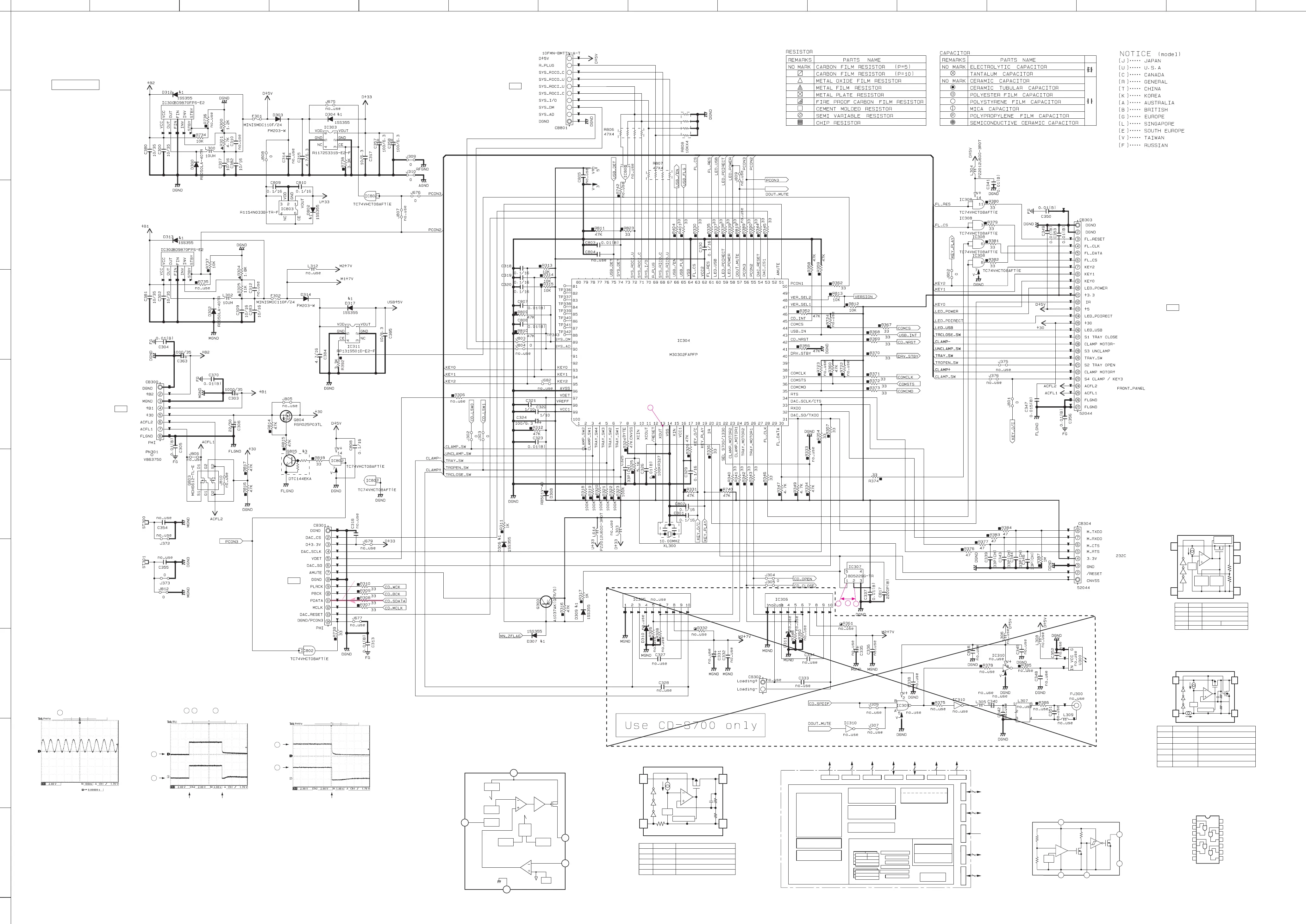
CD-1330
40
DIGITAL 2/3
IC304
CB801
IC305
CB301
CB300
IC311
IC302
IC300
IC303
IC803
IC802
IC802
IC802
IC802
IC306
IC307
IC309
IC310
IC310
CB304
CB303
IC308
IC308
IC308
IC308
IC310
4.9
4.2
4.9
4.9
3.3
3.3
0
4.2
4.2
0
4.2
0
20.0
20.0
4.9
0
1. 0
10.0
7. 9
7. 9
7. 9
7. 4
7. 4
0
0
7. 4
0
0
0
3.3
3.3
0
3.3
3.3
3.3
3.3
3.3
3.3
3.3
3.3
0
3.1
3.3
3.3
2.9
0
3.4
3.4
3.4
3.4
0
0
0
4.9
4.9
4.9
0
3.3
0
4.9
0
0
0
0
0
0
0
3.4
3.4
0
0
3.3
3.3
3.3
3.3
3.3
0
0
3.3
1. 7
0
1. 5
3.3
3.3
3.3
0
3.4
0
3.4
3.3
0
3.3
3.3
3.3
3.3
0
0
3.3
0
0
0
3.2
3.2
3.3
3.3
3.3
3.3
0
1. 6
3.3
3.3
0
3.3
3.3
3.3
0
0
0
3.3
3.3
0
0
20.0
20.0
7. 9
0
1. 1
20.0
AUDIO OUT
POINT C XL300 (Pin 13 of IC304)
C
12 pin
1 pin
2 pin
1 pin
2
1
2
Power ON Power OFF Power OFF
POINT D 1 / Pin2, 2 / Pin1 of IC307
D
1
2
MICROPROCESSOR
RESET IC
LEGULATOR
LEGULATOR
DC/DC CONVERTER
DC/DC CONVERTER
LEVEL
SHIFTER
DIGITAL (1)
IC304: M30302FAPFP
Single-chip 16-bit microprocessor
Timer (16-bit)
Peripheral function
Input (timer A) x3
Output (timer B) x3
Watchdog timer
(15-bit)
DMAC
(2-channel)
A/D converter
(10-bit
X
18-channel
)
System clock generator
X
IN
-X
OUT
X
CIN
-X
COUT
M16C/60 series
Microprocessor core
Port P0
8
Port P1
8
Port P2
8
Port P3
8
Port P4
8
Port P5
8
Port P6
8
8
R0LR0H
R1H R1L
R2
R3
ISP
USP
INTB
SB
CRC arithmetic circuit (CCITT)
(Polynomial : X
16
+X
12
+X
5
+1)
Multiplier
7
8
Port P9
8
Port P10
Port P8_5
Port P8
Port P7
Memory
ROM
(Note 1)
RAM
(Note 2)
FB
A1
FB
A1
A0
FLG
PC
UART or clock synchronous type
serial I/O
(3-channel)
Note 1: ROM contents vary depending on types.
RAM contents vary depending on types.
Note 2:
VDD
CE
Pin No.
1
2, 5
3
4
6
Symbol
V
OUT
GND
CE
NC
V
DD
Description
Output Pin of Voltage Regulator
Ground Pin
Chip Enable Pin
No Connection
Input Pin
Vref
61
3 2,5
Current Limit
VOUT
GND
IC303: R1172S331B-E2-F
CMOS-based positive-voltage regulator IC
IC308, 802: TC74VHCT08AFT
Quad 2-input AND gate
Vcc14
4B
4A
4Y
3B
3A
3Y
1A 1
2
3
13
12
11
10
9
8
4
5
6
7
1B
1Y
2A
2B
2Y
GND
VDD
CE
Pin No.
1
2
3
4
5
6
Symbol
V
OUT
GND
CE
NC
V
DD
Description
Output Pin of Voltage Regulator
Ground Pin
GND Ground Pin
Chip Enable Pin (“H” Active)
No Connection
Input Pin
Vref
16
2,54
Current Limit
VOUT
GND
IC311: RP131S501D-E2-F
Voltage regulator
OSC
PWM COMP DRIVER
STBY
STBY
OUT
INV
GND
VCC
TSD
OCP
Error AMP
SS
CTL
LOGIC
IC300, 302: BD9870FPS-E2
High stand voltage 1 channel step-down switching regulator
VREF
1
5
FIN
4
2
Vref
Vout
CT
GND
V
DD
NC
4
1
2
3
5
–
+
IC307: BD5229G-TR
Voltage detector IC with adjustable output delay
VDD
CE
3
1
5
Pin No. Symbol Description
1V
OUT
Output Pin for Voltage Regulator
GND Ground
V
DD
Power Supply Pin
CE
NC
Chip Enable Pin (active at "H")
B Version No Connection
2
3
4
5
2
V
OUT
4
NC
GND
IC803: R1154N033B-TR-F
Voltage regulator
Vref
Short
Protection
Circuit
Current
Limit
Circuit
Thermal
Shutdown
to OPERATION (4)_W201
Page 43
L5
to DIGITAL (2)_CB901
Page 41
J3
to OPERATION (3)_W1
Page 42
G6
to OPERATION (9)_CB151
Writing port
Page 43
F8
 Loading...