EasyManua.ls Logo

Yamaha Magicstomp UB99 User Manual

Yamaha Magicstomp UB99
33 pages
To Next Page IconTo Next Page
Page #1 background imageLoading...
Page #1 background image
UB99
1
SERVICE MANUAL
GA
011703
Copyright (c) Yamaha Corporation. All rights reserved. PDF-K244 ’03.11
HAMAMATSU, JAPAN
20031201-28000
CONTENTS
SPECIFICATIONS .................................................. 3
PANEL LAYOUT .................................... 4
BLOCK DIAGRAM ........................... 5
CIRCUIT BOARD LAYOUT ................. 6
DISASSEMBLY PROCEDURE .............................. 6
LSI PIN DESCRIPTION ................................ 8
IC BLOCK DIAGRAM ................................... 11
CIRCUIT BOARD .......................................... 12
INSPECTIONS / FACTORY SET
............................................ 14/18
BACKUP THE USER PATCH DATA
......................................... 22
ERROR MESSAGES ............................. 23
PARTS LIST
CIRCUIT DIAGRAM
GUITAR EFFECTS PROCESSOR
UB99
(目次)
(総合仕様)
(パネルレイアウト)
(ブロックダイアグラム)
(ユニットレイアウト)
(分解手順)
(LSI端子機能表)
(ICブロック図)
(シート基板図)
(検査/ファクトリーセット)
(ユーザーパッチのバックアップ)
(エラーメッセージ)
(回路図)
Question and Answer IconNeed help?

Do you have a question about the Yamaha Magicstomp UB99 and is the answer not in the manual?

Yamaha Magicstomp UB99 Specifications

General IconGeneral
A/D Conversion24-bit
D/A Conversion24-bit
Sampling Frequency44.1 kHz
Presets99
Outputs2 x 1/4" (L/Mono, R)
TypeMulti-effects
EffectsReverb, Delay, Distortion
Inputs1 x 1/4\" (Instrument)
MIDIIn/Out
Power SupplyAC adapter

Summary

Important Notice

Specifications

Panel Layout

Top Panel

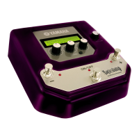
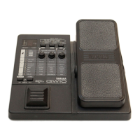
Diagram and labels for the top surface controls and display.

Rear Panel

Diagram and labels for the rear panel connectors and switches.

Block Diagram

Circuit Board Layout

Bottom View

Shows the component layout on the bottom side of the main circuit board.

Disassembly Procedure

Bottom Case Removal

Steps to remove the bottom case of the unit.

Rear Panel Removal

Steps to detach the rear panel and its associated parts.

DM Circuit Board Removal

Instructions for removing the main circuit board (DM).

Foot Switch Removal

Procedure for removing the foot switch assembly.

LSI Pin Description

IC Block Diagrams

Circuit Board Diagram

DM Circuit Board Diagram

Detailed schematic layout of the main circuit board (DM).

Inspections and Factory Set

Preparation

Required instruments, jigs, and terminal connections for testing.

Measurement Conditions

Specifies conditions for input signals, knob settings, and instrument impedance.

Method of Inspection

Details how to enter TEST MODE and perform various checks.

Backup User Patch Data

Error Messages

Parts List

Overall Assembly Parts

List of parts for the complete unit assembly.

Top Case Assembly Parts

List of components specific to the top case assembly.

Electrical Parts

List of electronic components used in the unit.

Related product manuals