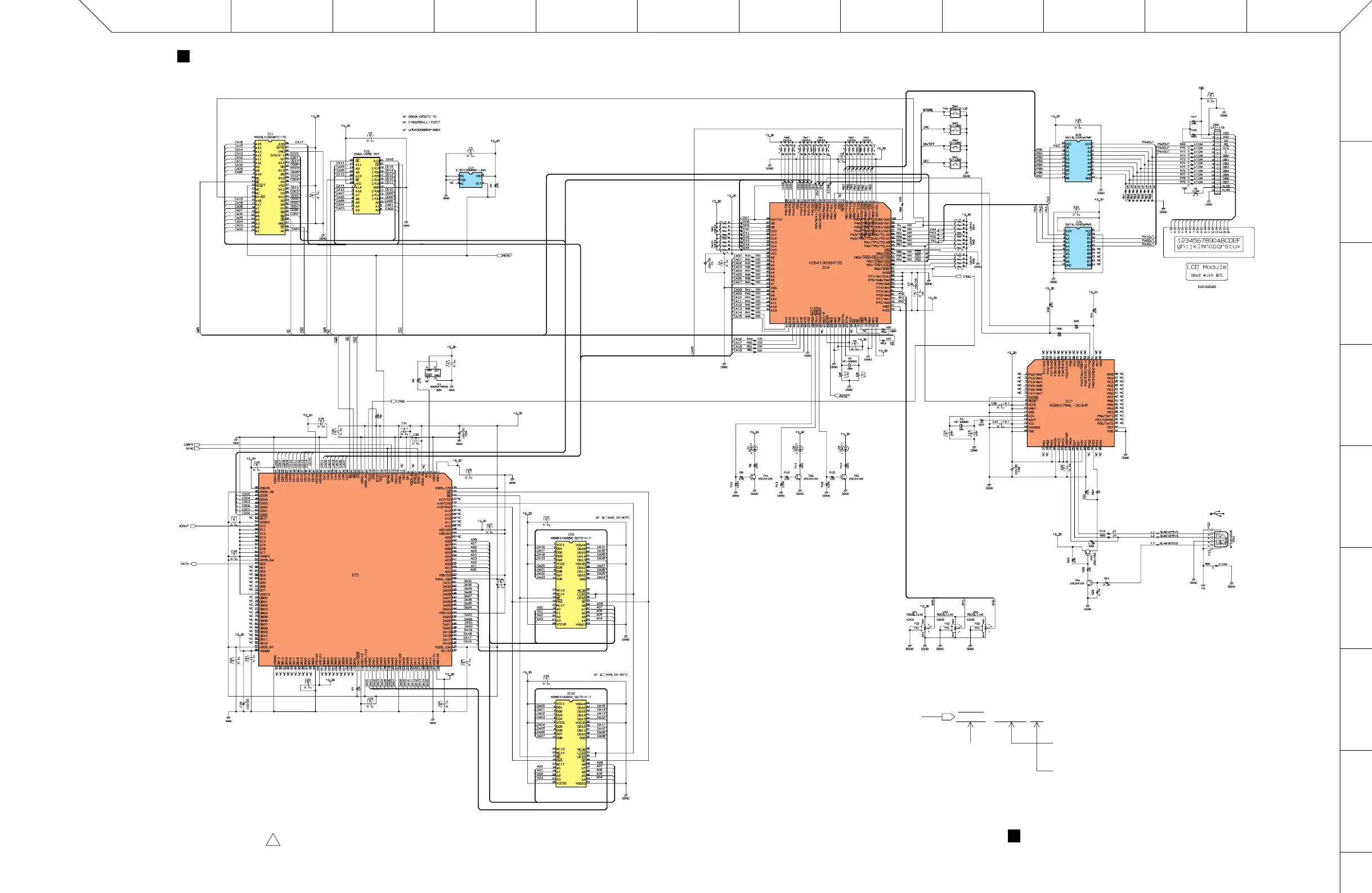
1
2
3
4
5
6
7
8
L
KJIHGFEDCBA
UB99 DM CIRCUIT DIAGRAM 1/2
DIC-00001-2
3
UB99 DM CIRCUIT DIAGRAM 1/2
UB99
1
RESET
(シート間コネクタの読み方について)
(ページNo.は信号の行先ページを示します。)
(回路図表記上の注意)
Notation for Circuit Diagrams
1. How to identify inter-sheet connectors
The page number indicates the destination page.
対応するシート間のコネクタのあるロケーションを示します。
(アルファベットが水平方向、数字が垂直方向)
This indicates the location of the counter inter-sheet connector.
(The alphabet indicates horizontal direction and the number
indicates vertical direction)
to page 1: G4
Signal name
(信号名)
FLASH ROM 16M
PROGRAM
SYSTEM
RESET
CPU (MAIN)
DRAM 4M
DSP 6
CPU (USB)
DRAM 4M
TRANSCEIVER
TRANSCEIVER
SRAM 256K
to Page 1: G4
to Page 2: H3
from Page 2: C5
from Page 2: F5
from Page 2: G3
to Page 2: G4
from Page 1: D3
from Page 2: H3
: Ceramic Capacitor
(セラミックコンデンサー)(
セ
)
: Metal Oxide Film Resistor
(酸化金属被膜抵抗)
酸金
YSS910-V (DSP6)
YSS910-S (DSP6)or
(USB)
STORE
+
-
ON / OFF
-
+
ON / OFF
CONTROL 1
CONTROL 2
CONTROL 3
DSP