1
2
3
4
5
6
7
8
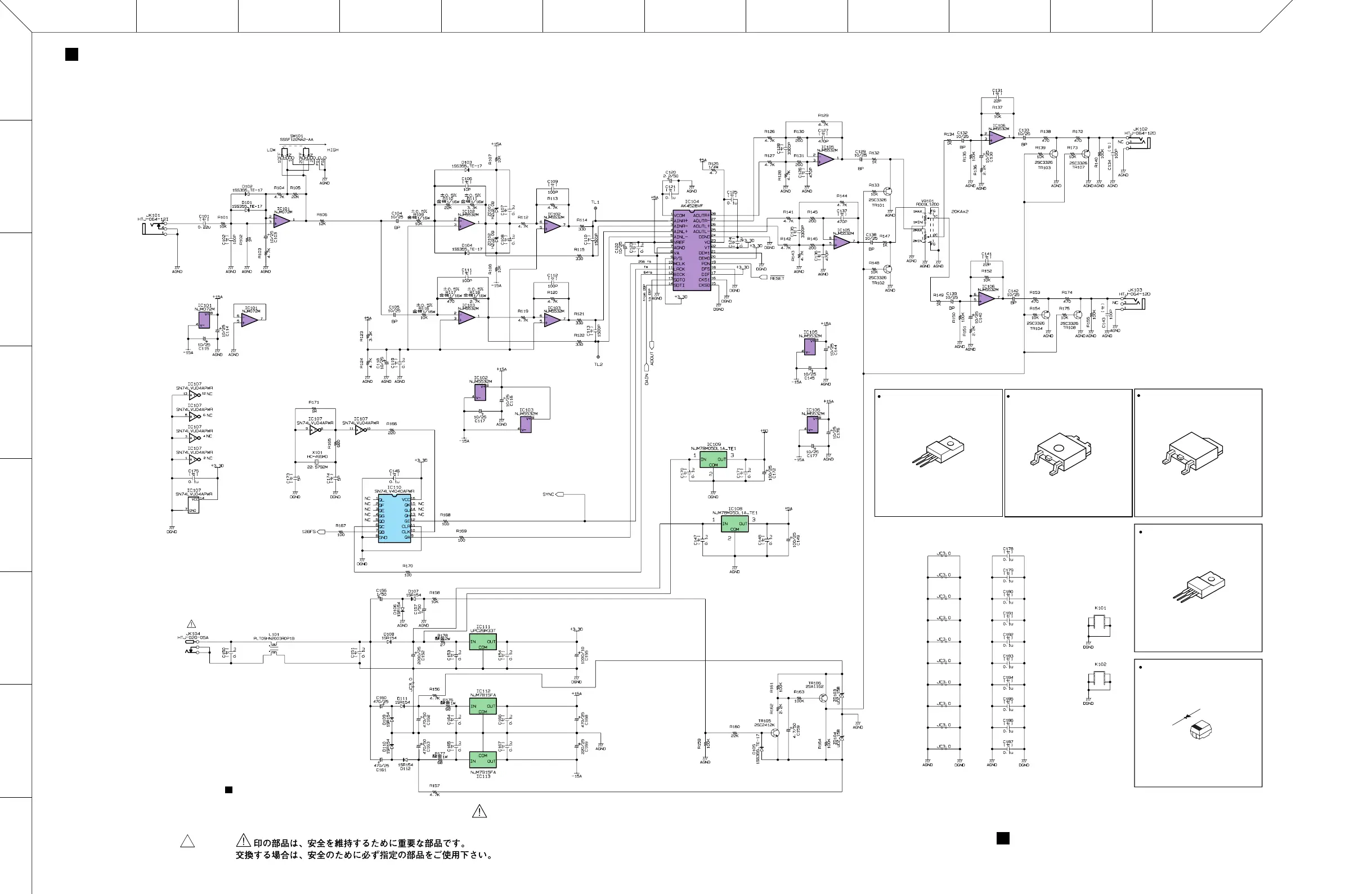
UB99 DM CIRCUIT DIAGRAM 2/2
DIC-00001-3
2
2
UB99 DM CIRCUIT DIAGRAM 2/2
UB99
LKJIHGFEDCBA
INPUT
OP AMP
OP AMP
ADC/DAC
OP AMP
OP AMP
OP AMP
OP AMP
OP AMP
OP AMP
REGULATOR +5V
REGULATOR +5V
REGULATOR +3.3V
REGULATOR +15V
REGULATOR -15V
OP AMP
OP AMP
INVERTER
BINARY
COUNTER
to Page 1: A4
to Page 1: A5
from Page 1: A6
to Page 1: A5
from Page 1: D3
OUTPUT R
INPUT LEVEL
AC IN
OUTPUT L/MONO
: Ceramic Capacitor
(セラミックコンデンサー)(
セ
)
: Metal Oxide Film Resistor
(酸化金属被膜抵抗)
酸金
1SR154-400
(
VT532500
)
DIODE
DM: D106-112
1: ANODE
2: CATHODE
2
1
NJM7915FA(XD854A00)
REGULATOR -15V
DM: IC113
1
2
3
1: OUTPUT
2: INPUT
3: COMMON
: Carbon Resistor (chip)
(チップ
抵抗
)金被1/16W
NJM7815FA(XD853A00)
REGULATOR +15V
DM: IC112
1
2
3
1: OUTPUT
2: COMMON
3: INPUT
NJM78M05DLA(XS534A00)
REGULATOR +5V
DM: IC108, 109
1: INPUT
2: GND
3: OUTPUT
1
2
3
µPC29M33T-E1(XU965A00)
REGULATOR +3.3V
DM: IC111
1: INPUT
2: COMMON
3: OUTPUT
1
2
3
VOLUME
MUTE
Components having special characteristics are marked and must be replaced
with parts having specifications equal to those originally installed.
TO SERVICE PERSONNEL
Critical Components Information