26
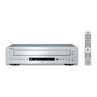
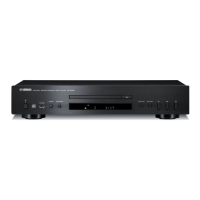
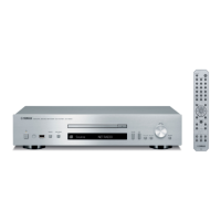
CD-1330
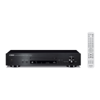
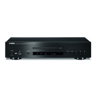
CD-1330
No. Port Name Function Name Detail of Function
1 N.C.
2 USBNOC USB over-current input (negative polarity)
3 USBNPP USB, VBUS power output control terminal (negative polarity)
4 USBD- USB D- terminal
5 VSS AVSS Ground / Analog power supply for USB / Connect to VSS.
6 USBD+ USB D+ terminal
7 AVDD Analog power supply for USB / Connect to VDD33.
8 N.C.
9 VDD3 VDD33
Power for on-chip regulator (2.7V to 3.6V)
I/O power supply (2.7V to 3.6V)
10 VDDI VDD18/VOUT
Power for internal circuit (1.8V t±0.15V)
Connect all VDD18 terminals outside of chip.
Also, connect a 10μF capacitor between VDD18 and VSS of No.10 pin and place it
near LSI.
On-chip regulator output (1.8V ±0.15V)
11 OSCI
High-speed oscillation input terminal (fosc)
(When PLL used: 6.33 MHz to 20 MHz)
12 OSCO High-speed oscillation output terminal
13 VSS Ground
14 NRST Reset signal input terminal (negative polarity)
15 MMOD0 Operation mode setting terminal
16 MMOD1 Operation mode setting terminal
17 VPP Power for rewriting built-in Flash memory (3.3V ±0.3V) / only for Flash built in model
18 OCD_SDA Clock, data input/output terminal for on-chip debugger
19 OCD_SCL Clock, data input/output terminal for on-chip debugger
20
N.C.
21
22
23
24
25 USB_IN General purpose input/output port 0
26
N.C.
27
28
29
30
31
32
33
34
35
36
37
38 VDD3 VDD33
Power for on-chip regulator (2.7V to 3.6V)
I/O power supply (2.7V to 3.6V)
39 N.C.
40 VSS Ground
41 N.C.
42 VDDI VDD18
Power supply for internal circuit (1.8V ±0.15V)
Connect all VDD18 terminals outside of chip.
Also, connect a 10μF capacitor between VDD18 and VSS of No.10 pin and place it
near LSI.
43
N.C.44
45
46 I2C_SCL P35/SCL3 General purpose input/output port 3
47 N.C.
48 I2C_SDA P33/SDA3 General purpose input/output port 3
49 VDD3 VDD5 I/O power supply (5V type I/O)
50 N.C.
 Loading...