ZXRAN V9200 Product Description
ZTE Confidential & Proprietary 3
FIGURES
Figure 1- 1 V9200 in the GSM/UMTS/LTE/NB-IoT/5G Multi-mode Network
.............................
6
Figure 1- 2 Indoor Scenario: V9200 and RRUs Integrated in L-Rack-I1
....................................
8
Figure 1- 3 Outdoor Scenario: V9200 in BS9900A Connected to RRUs/AAUs Nearby
..........
8
Figure 1- 4 Centralized Deployment Scenario: V9200 in V9810 Connected to RRUs/AAUs
Faraway
...................................................................................................................................................
9
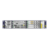
Figure 2- 1 Appearance of V9200
..................................................................................................
10
Figure 2- 2 Hardware Architecture of V9200
................................................................................
11
Figure 2- 3 VSWc0 Panel
................................................................................................................
12
Figure 2- 4 VSWc2 Panel
................................................................................................................
12
Figure 2- 5 VSWd1 Panel
................................................................................................................
12
Figure 2- 6 VSWd2 Panel
................................................................................................................
12
Figure 2- 7 VBPc0 Panel
.................................................................................................................
16
Figure 2- 8 VBPc1 Panel
.................................................................................................................
18
Figure 2- 9 VBPc5 Panel
.................................................................................................................
19
Figure 2- 10 VBPc7 Panel
...............................................................................................................
20
Figure 2- 11 VBPd0 Panel
...............................................................................................................
21
Figure 2- 12 VBPd1 Panel
...............................................................................................................
23
Figure 2- 13 VBPd2 Panel
...............................................................................................................
24
Figure 2- 14 VEMc1 Panel
..............................................................................................................
25
Figure 2- 15 VEMc2 Panel
..............................................................................................................
25
Figure 2- 16 VEMc4 Panel
..............................................................................................................
26
Figure 2- 17 VPDc1 Panel
...............................................................................................................
27
Figure 2- 18 VFC1 Panel
.................................................................................................................
28
Figure 4- 1 Appearance of BS9900A (VC9910A + PC9910A)
..................................................
32
Figure 4- 2 Internal Structure of VC9910A (with ZXDU68 B201)
..............................................
33
Figure 4- 3 Internal Structure of the VC9910A (with ZXDU68 B351)
.......................................
33
Figure 4- 4 Internal Structure of PC9910A
....................................................................................
34
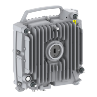
Figure 4- 5 Appearance of BS8906B
.............................................................................................
35
 Loading...