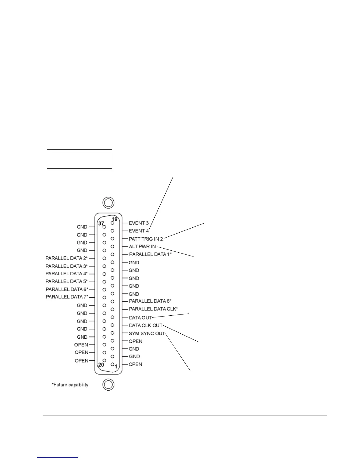
5. AUXILIARY I/O
ALT PWR IN: Used with an internal baseband
generator. This pin accepts a CMOS signal for
synchronization of external data and alternate power
signal timing. Damage levels are > +8 V and < −4 V.
View looking into
rear panel connector
DATA CLK OUT: Used with an internal baseband
generator. This pin relays a CMOS bit clock signal for
synchronizing serial data.
DATA OUT: Used with an internal baseband generator.
This pin outputs data (CMOS) from the internal data
generator or the externally supplied signal at data input.
EVENT 3: Used with an internal baseband generator. In arbitrary waveform mode,
this pin outputs a timing signal generated by Marker 3. A marker (3.3 V CMOS
high for both positive and negative polarity) is output on this pin when a Marker 3 is
turned on in the waveform. Reverse damage levels: > +8 V and < −4 V.
PATT TRIG IN 2: Accepts a signal that triggers an
internal pattern or frame generator to start single
pattern output. Minimum pulse width: 100 ns.
Damage levels: > +5.5 V and < −0.5 V.
SYM SYNC OUT: Used with an internal baseband
generator. This pin outputs the CMOS symbol clock for
symbol synchronization, one data clock period wide.
EVENT 4: Used with an internal baseband generator. In arbitrary
waveform mode, this pin outputs a timing signal generated by
Marker 4. A marker (3.3V CMOS high for both positive and
negative polarity) is output on this pin when a Marker 4 is turned
on in the waveform. Reverse damage levels: > +8 V and < −4 V.
 Loading...