3
TABLE OF CONTENTS
1. GENERAL
Connections ............................................................................. 4
2. DISASSEMBLY
2-1. Sub Panel Assy .................................................................... 7
2-2. CD Mechanism Block ......................................................... 7
2-3. Main Board Section ............................................................ 8
2-4. Main Board ......................................................................... 8
2-5. Heat Sink (CT) .................................................................... 9
2-6. Sub Board............................................................................ 9
2-7. Servo Board....................................................................... 10
2-8. Floating Block Assy .......................................................... 10
2-9. Lever Assy (CD Up Holder).............................................. 11
2-10. Lever (CD Roller) Sub Assy ............................................. 11
2-11. Lever Assy (CD Holder) ................................................... 12
2-12. Motor (Sled) Sub Assy ...................................................... 12
2-13. Pick-up Sub Assy .............................................................. 13
3. ELECTRICAL ADJUSTMENT.................................... 14
4. DIAGRAMS
4-1. IC Pin Descriptions ........................................................... 15
4-2. Block Diagram –CD Section–........................................... 19
4-3. Block Diagram –Main Section–........................................ 20
4-4. Block Diagram –Front Section–........................................ 21
4-5. Circuit Boards Location .................................................... 21
4-6. Printed Wiring Boards –CD Mechanism Section–............ 22
4-7. Schematic Diagram –CD Mechanism Section– ................ 24
4-8. Printed Wiring Board –Main Section– .............................. 25
4-9. Schematic Diagram –Main Section (1/2)– ........................ 26
4-10. Schematic Diagram –Main Section (2/2)– ........................ 27
4-11. Printed Wiring Boards –Front Section– ............................ 28
4-12. Schematic Diagram –Front Section– ................................ 29
4-13. IC Block Diagrams............................................................ 30
5. EXPLODED VIEWS
5-1. Chassis Section ................................................................. 32
5-2. Front panel Section ........................................................... 33
5-3. CD Mechanism Section (1) ............................................... 34
5-4. CD Mechanism Section (2) ............................................... 35
6. ELECTRICAL PARTS LIST ........................................ 36
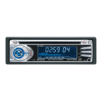
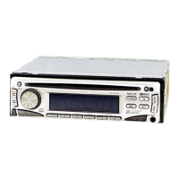
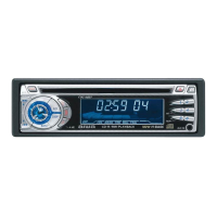
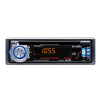
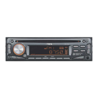
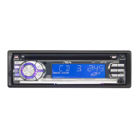
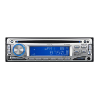
CDC-R237
 Loading...