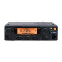
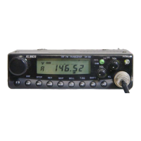
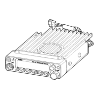
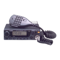
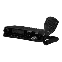
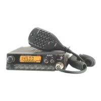
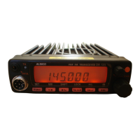
DR-140T/E/TE1/TE2
Service Manual
C O N T E N T S
• SPECIFICATIONS
1) G eneral................................................................................2
2) Transm itter................*
........................................................
2
3) Receiver...............................................................................3
• CIRCUIT DESCRIPTION
1) Receiver S yte m
......................................................... 4 -5
2) Transmitter System ....................................................5-6
3) PLL Circuit.........................................................................6
4) Terminal Function of C PU ........................................... 7
• SEMICONDUCTOR D ATA
1) AK2341
.
...........................................................................10
2) AN78L05M ................................................................... 11
3) LA4425A..........................................................................11
4) M 5218 FP .........................................................................11
5) M 56760FP...................................................................... 12
6) M 67746............................................................................13
7) M 68702H..........................................................................13
6) M 68702L..........................................................................13
9) MC7808CT...................................................................... 14
10) RH5VL32AA-T1 ............................................................14
11) RH5VL45AA-T1 ............................................................14
12) TK10930VTL...................................................................15
13) jczPC2710T...................................................................... 16
1 4 )24LC16B 16
15)
.
Transistor,Diode and LED Outline D raw ings
.......
17
16) L C D ....................................................................................18
• EXPLODED VIEW
1) Bottom V ie w
...................................................................19
2) LCD Assem bly...............................................................20
3) Top, and Front View .....................................................21
• PARTS LIST
Main Unit...................................................................... 21-22
Packing.................................................................................23
CPU Unit...............................................................................23
SP Unit ................................................
.
.............................
23
VCO U nit.............................................................................23
Mechanical P arts..............................................................23
EJ-20U .................................................................................24
• AD JUSTM EN T
1) Required Test Equipm ent
..........................................
25
2) PLL Adjustm ent.............................................................26
3) TX A djustm ent
.........
.
...................................................26
4) RX Adjustment......
.
.......................................................27
5) Adjustm ent Points
........................................................28
• PC BOAD VIEW
1) Main Unit Side A ...........................................................29
2) Main Unit Side B...........................................................30
3) CPU Unit Side A ..........................................................31
4) CPU Unit Side B............................................................31
5) VCO Unit Side A ...........................................................32
6) VCO Unit Side B ...........................................................32
7) EJ-20U (CTCSS Unit: O ption)..................................33
• BLO CK D IA G R A M ...................................................................34
• SCHEMATIC DIAGRAM
1) Main Unit T/E ....................................................
.....
35 -3 6
2) Main Unit T E 1/TE 2...............................................37-38
3) CPU U n it
........................................................................
39
4) VCO U nit
.............
.
..........................................................40
5) EJ-20U (CTCSS Unit: Option)
...............................
41
ALINCO, in c