EasyManua.ls Logo

Alinco DR-140TE2 User Manual

Alinco DR-140TE2
43 pages
To Next Page IconTo Next Page
Page #1 background imageLoading...
Page #1 background image
DR-140T/E/TE1/TE2
Service Manual
C O N T E N T S
SPECIFICATIONS
1) G eneral................................................................................2
2) Transm itter................*
........................................................
2
3) Receiver...............................................................................3
CIRCUIT DESCRIPTION
1) Receiver S yte m
......................................................... 4 -5
2) Transmitter System ....................................................5-6
3) PLL Circuit.........................................................................6
4) Terminal Function of C PU ........................................... 7
SEMICONDUCTOR D ATA
1) AK2341
.
...........................................................................10
2) AN78L05M ................................................................... 11
3) LA4425A..........................................................................11
4) M 5218 FP .........................................................................11
5) M 56760FP...................................................................... 12
6) M 67746............................................................................13
7) M 68702H..........................................................................13
6) M 68702L..........................................................................13
9) MC7808CT...................................................................... 14
10) RH5VL32AA-T1 ............................................................14
11) RH5VL45AA-T1 ............................................................14
12) TK10930VTL...................................................................15
13) jczPC2710T...................................................................... 16
1 4 )24LC16B 16
15)
.
Transistor,Diode and LED Outline D raw ings
.......
17
16) L C D ....................................................................................18
EXPLODED VIEW
1) Bottom V ie w
...................................................................19
2) LCD Assem bly...............................................................20
3) Top, and Front View .....................................................21
PARTS LIST
Main Unit...................................................................... 21-22
Packing.................................................................................23
CPU Unit...............................................................................23
SP Unit ................................................
.
.............................
23
VCO U nit.............................................................................23
Mechanical P arts..............................................................23
EJ-20U .................................................................................24
AD JUSTM EN T
1) Required Test Equipm ent
..........................................
25
2) PLL Adjustm ent.............................................................26
3) TX A djustm ent
.........
.
...................................................26
4) RX Adjustment......
.
.......................................................27
5) Adjustm ent Points
........................................................28
PC BOAD VIEW
1) Main Unit Side A ...........................................................29
2) Main Unit Side B...........................................................30
3) CPU Unit Side A ..........................................................31
4) CPU Unit Side B............................................................31
5) VCO Unit Side A ...........................................................32
6) VCO Unit Side B ...........................................................32
7) EJ-20U (CTCSS Unit: O ption)..................................33
BLO CK D IA G R A M ...................................................................34
SCHEMATIC DIAGRAM
1) Main Unit T/E ....................................................
.....
35 -3 6
2) Main Unit T E 1/TE 2...............................................37-38
3) CPU U n it
........................................................................
39
4) VCO U nit
.............
.
..........................................................40
5) EJ-20U (CTCSS Unit: Option)
...............................
41
ALINCO, in c
Question and Answer IconNeed help?

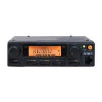
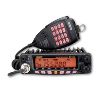
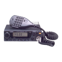
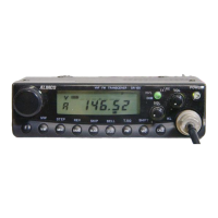
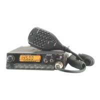
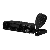
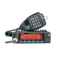
Do you have a question about the Alinco DR-140TE2 and is the answer not in the manual?

Alinco DR-140TE2 Specifications

General IconGeneral
ModeFM
Voltage13.8 V DC ±15%
Dimensions140 x 40 x 180 mm
Channels / memory management200 channels
Antenna ConnectorSO-239
Weight1 kg

Summary

Specifications

General Specifications

Describes general technical parameters including frequency ranges, memory channels, and display capabilities.

Transmitter Specifications

Details transmitter output power, emission type, modulation system, and frequency deviation.

Receiver Specifications

Details receiver system, IF frequencies, sensitivity, selectivity, and audio output.

Circuit Description

Receiver System Circuit Description

Explains the signal path and components within the receiver circuit, from antenna to AF signal.

Transmitter System Circuit Description

Explains the signal path and components within the transmitter circuit, from microphone to RF output.

PLL Circuit Description

Describes the Phase-Locked Loop circuit, including its summary, reference oscillator, loop filter, and VCO.

Semiconductor Data

AK2341 CTCSS Encoder/Decoder Data

Provides pinout, function table, and block diagram for the AK2341 CTCSS encoder/decoder IC.

AN78L05M 5V Voltage Regulator Data

Details the specifications and test circuit for the AN78L05M 5V voltage regulator.

LA4425A 5W Audio Power Amplifier Data

Presents the test circuit and specifications for the LA4425A 5W audio power amplifier IC.

M5218FP Dual Low Noise Op-Amp Data

Shows the pinout and configuration for the M5218FP dual low noise operational amplifier.

M56760FP Frequency Synthesizer Data

Describes the pinout, function table, and block diagram of the M56760FP frequency synthesizer.

M67746 RF Power Module Data

Provides ratings and specifications for the M67746 60W RF power module (144-148MHz).

M68702H RF Power Module Data

Provides ratings and specifications for the M68702H 60W RF power module (150-175MHz, TE2).

M68702L RF Power Module Data

Provides ratings and specifications for the M68702L 60W RF power module (135-160MHz, TE1).

MC7808CT 8V Voltage Regulator Data

Details the test circuit for the MC7808CT 8V voltage regulator.

RH5VL32AA-T1 Voltage Detector Data

Shows the equivalent circuit for the RH5VL32AA-T1 C-MOS voltage detector.

RH5VL45AA-T1 Voltage Detector Data

Shows the equivalent circuit for the RH5VL45AA-T1 C-MOS voltage detector.

TK10930VTL FM IF IC Data

Provides circuit diagram, parameters, and ratings for the TK10930VTL narrow band FM IF IC.

μPC2710T RF Amplifier Data

Lists parameters, test circuit, and block diagram for the μPC2710T RF amplifier.

24LC16B Serial EEPROM Data

Details the block diagram, pin names, and descriptions for the 24LC16B EEPROM.

Transistor, Diode, LED Outline Drawings

Illustrates outline drawings and pinouts for various transistors, diodes, and LEDs.

LCD Display Data

Shows LCD patterns and the connection table for display segments.

Exploded View

Bottom View Exploded

Illustrates the components and screw torque for the bottom of the unit.

LCD Assembly Exploded

Shows the assembly breakdown of the LCD unit.

Top and Front Views Exploded

Depicts exploded views of the top and front sections of the device.

Parts List

Main Unit Parts List

Lists all parts for the main unit with their corresponding numbers and descriptions.

Packing Parts List

Lists accessories and packaging materials included with the product.

CPU Unit Parts List

Lists components specific to the CPU unit.

SP Unit Parts List

Lists components for the Speaker unit.

VCO Unit Parts List

Lists components for the Voltage Controlled Oscillator unit.

Mechanical Parts List

Lists mechanical components such as knobs, cases, and screws.

EJ-20U Parts List

Lists components for the optional EJ-20U CTCSS unit.

Adjustment Procedures

Required Test Equipment

Lists necessary equipment for performing adjustments and tests.

PLL Adjustment

Provides steps and parameters for adjusting the Phase-Locked Loop circuit.

TX Adjustment

Details the procedure for adjusting transmitter output power and deviation.

RX Adjustment

Outlines the steps for tuning receiver sensitivity and squelch level.

Adjustment Points Diagram

Shows a diagram indicating the physical locations of adjustment components on the PCB.

PC Board View

Main Unit Side A PCB View

Shows the component layout for the Main Unit's Side A.

Main Unit Side B PCB View

Shows the component layout for the Main Unit's Side B.

CPU Unit Side A PCB View

Illustrates the component placement on the CPU Unit's Side A.

CPU Unit Side B PCB View

Illustrates the component placement on the CPU Unit's Side B.

VCO Unit Side A PCB View

Depicts the component layout for the VCO Unit's Side A.

VCO Unit Side B PCB View

Depicts the component layout for the VCO Unit's Side B.

EJ-20U (CTCSS Unit) PCB View

Shows the component layout for the optional EJ-20U unit.

Block Diagram

Schematic Diagrams

Main Unit T/E Schematic

Provides the detailed schematic for the Main Unit (T/E versions).

Main Unit TE1/TE2 Schematic

Provides the detailed schematic for the Main Unit (TE1/TE2 versions).

CPU Unit Schematic

Presents the schematic diagram for the CPU Unit.

VCO Unit Schematic

Shows the schematic diagram for the VCO Unit.

EJ-20U (CTCSS Unit: Option) Schematic

Displays the schematic for the optional EJ-20U CTCSS unit.

Related product manuals