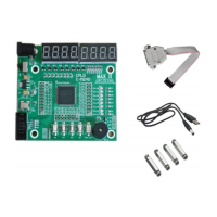
Thank you for choosing as the hurricane core development board - learning board
www.sz-21eda.com
Translated without permission by organicmonkeymotion.wordpress.com V1 11/01/2014
3
Development board intended use
The development board uses the Altera's MAX II Series EP M240 T100C5N chip design. This
chip is also compatible with EP M 570T100C5N.
The objective of this development board is the help customers reduce costs and accelerate learning
by providing quick access to programmable logic device design and development. Thus, this
development board provides a platform to help users quickly learn the hardware programmable
logic devices.
The development board provides a JTAG interface for programming the chip. Programming by
ByteBlasterII download cable is recommended is it can download to FPGA / CPLD chips by
Altera Corporation.
The development board has 65 I / O ports are cited by pin outs marked on the board. The user
can configure the pin assignments.
The development board facilitates user’s development of their own products. It also maximizes
savings for the user when studying the development costs.
Development board hardware description
MAX II U1 EP M240T100C5
8 7 segment LED displays
8 LED lights
BELL
Five separate keys
JTAG download mode
External 5V DC power supply
50MHz Active Crystals

 Loading...