Figure 2-16: PLL External Clock Output
C0
C1
C2
C4
C3
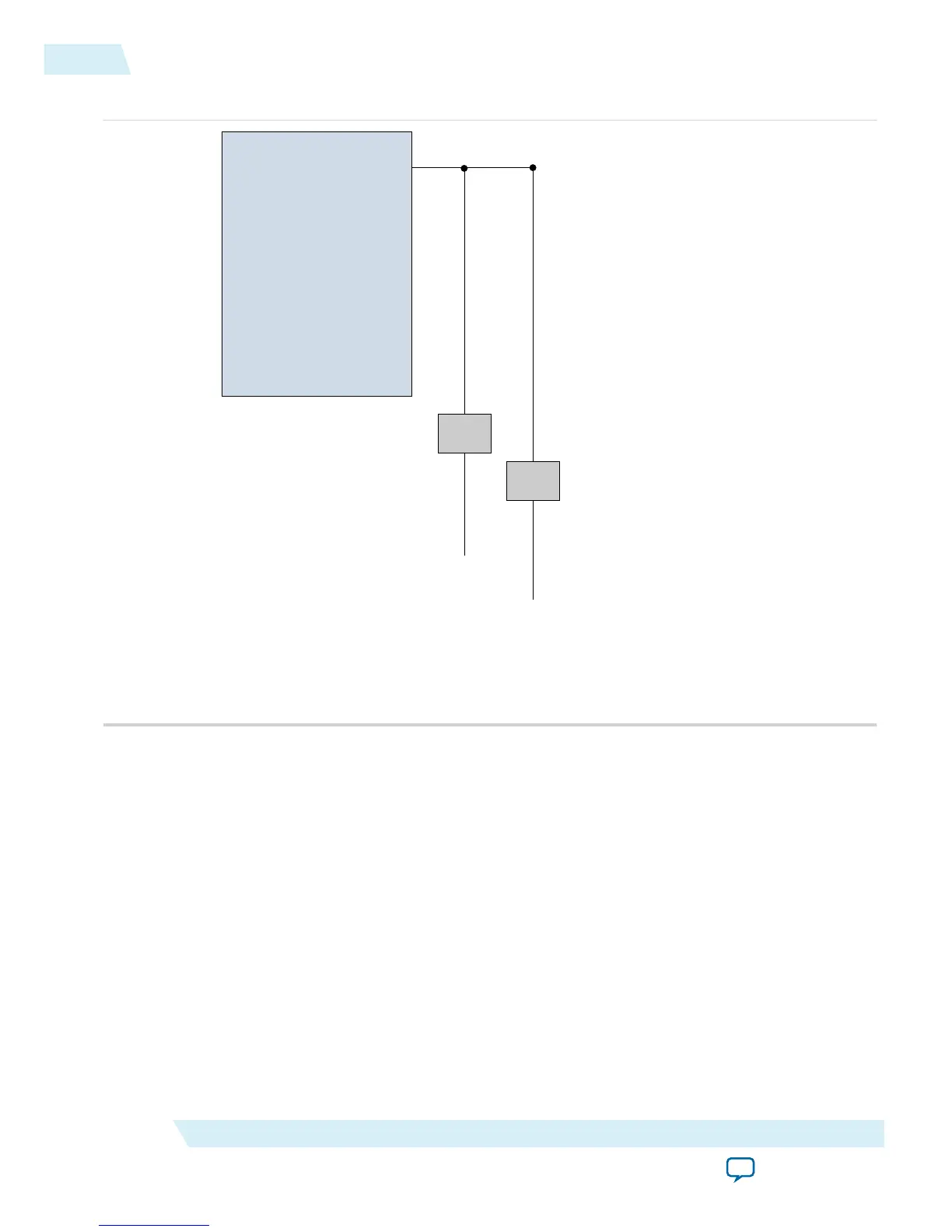
PLL #
clkena 1 (1)
clkena 0 (1)
PLL #_CLKOUTp (2)
PLL #_CLKOUTn (2)
Notes:
(1) These external clock enable signals are available only when using the ALTCLKCTRL IP core.
(2) PLL#_CLKOUTp and PLL#_CLKOUTn pins are dual-purpose I/O pins that you can use as one single-ended
or one differential clock output.
Each pin of a differential output pair is 180° out of phase. To implement the 180° out-of-phase pin in a
pin pair, the Quartus II software places a NOT gate in the design into the I/O element.
The clock output pin pairs support the following I/O standards:
• Same I/O standard as the standard output pins (in the top and bottom banks)
• LVDS
• LVPECL
• Differential high-speed transceiver logic (HSTL)
• Differential SSTL
The MAX 10 PLLs can drive out to any regular I/O pin through the GCLK. You can also use the external
clock output pins as general-purpose I/O pins if you do not require any external PLL clocking.
Related Information
MAX 10 General Purpose I/O User Guide
Provides more information about the I/O standards supported by the PLL clock output pins.
2-18
PLL External Clock Output
UG-M10CLKPLL
2015.06.12
Altera Corporation
MAX 10 Clocking and PLL Architecture and Features
Send Feedback