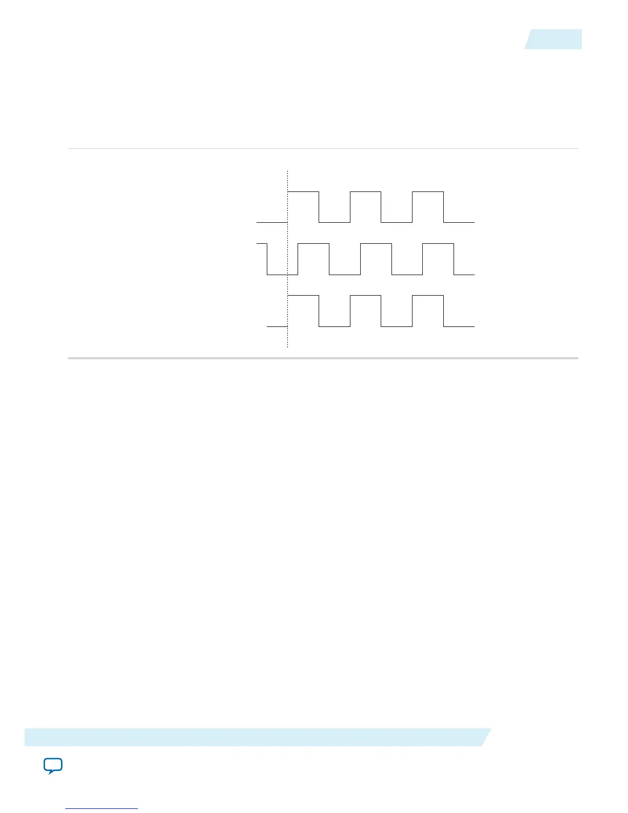
Zero-Delay Buffer Mode
In zero-delay buffer (ZDB) mode, the external clock output pin is phase-aligned with the clock input pin
for zero delay through the device. When using this mode, use the same I/O standard for the input clock
and output clocks to ensure clock alignment at the input and output pins.
Figure 2-15: Example of Phase Relationship Between the PLL Clocks in ZDB Mode
PLL Reference Clock
at the Input Pin
PLL Clock
at the Register Clock Port
External PLL Clock Output
at the Output Pin
Phase Aligned
PLL External Clock Output
Each PLL in the MAX 10 devices supports one single-ended clock output or one differential clock output.
Only the C0 output counter can feed the dedicated external clock outputs without going through the
GCLK. Other output counters can feed other I/O pins through the GCLK.
UG-M10CLKPLL
2015.06.12
Zero-Delay Buffer Mode
2-17
MAX 10 Clocking and PLL Architecture and Features
Altera Corporation
Send Feedback