EasyManua.ls Logo

Altera tPad DE2-115 - 3.4 Using 5-Megapixel Digital Image Sensor Module

Altera tPad DE2-115
43 pages
Print Icon
To Next Page IconTo Next Page
To Previous Page IconTo Previous Page
Loading...
15
LCD_R2
PIN_R28
LCD red data bus bit 2
2.5V
LCD_R3
PIN_U27
LCD red data bus bit 3
2.5V
LCD_R4
PIN_U28
LCD red data bus bit 4
2.5V
LCD_R5
PIN_V27
LCD red data bus bit 5
2.5V
LCD_G0
PIN_P21
LCD green data bus bit 0
2.5V
LCD_G1
PIN_R21
LCD green data bus bit 1
2.5V
LCD_G2
PIN_R22
LCD green data bus bit 2
2.5V
LCD_G3
PIN_R23
LCD green data bus bit 3
2.5V
LCD_G4
PIN_T21
LCD green data bus bit 4
2.5V
LCD_G5
PIN_T22
LCD green data bus bit 5
2.5V
LCD_B0
PIN_V28
LCD blue data bus bit 0
2.5V
LCD_B1
PIN_U22
LCD blue data bus bit 1
2.5V
LCD_B2
PIN_V22
LCD blue data bus bit 2
2.5V
LCD_B3
PIN_V25
LCD blue data bus bit 3
2.5V
LCD_B4
PIN_L28
LCD blue data bus bit 4
2.5V
LCD_B5
PIN_J26
LCD blue data bus bit 5
2.5V
LCD _DEN
PIN_P25
LCD RGB data enable
2.5V
TOUCH _PENIRQ_N
PIN_L22
AD7843 pen interrupt
2.5V
TOUCH _DOUT
PIN_L21
AD7843 serial interface data out
2.5V
TOUCH _BUSY
PIN_U26
AD7843 serial interface busy
2.5V
TOUCH _DIN
PIN_U25
AD7843 serial interface data in
2.5V
TOUCH _CS_N
PIN_T26
AD7843 serial interface chip select input
2.5V
TOUCH _DCLK
PIN_T25
AD7843 interface clock
2.5V
3
3
.
.
4
4
U
U
s
s
i
i
n
n
g
g
5
5
-
-
M
M
e
e
g
g
a
a
p
p
i
i
x
x
e
e
l
l
D
D
i
i
g
g
i
i
t
t
a
a
l
l
I
I
m
m
a
a
g
g
e
e
S
S
e
e
n
n
s
s
o
o
r
r
M
M
o
o
d
d
u
u
l
l
e
e
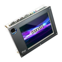
The tPad is equipped with a 5-Megapixel digital image sensor module that provides an active
imaging array of 2,592H x 1,944V. It features low-noise CMOS imaging technology that achieves
CCD image quality. In addition, it incorporates sophisticated camera functions on-chip such as
windowing, column and row skip mode, and snapshot mode.
The sensor can be operated in its default mode or programmed by the user through a simple
two-wire serial interface for frame size, exposure, gain settings, and other parameters. Table 3-3
contains the pin names and descriptions of the image sensor module.
Table 3-3 Pin assignment of the CMOS sensor
Signal Name
FPGA Pin No.
Description
I/O Standard
CAMERA_ PIXCLK
PIN_J27
Pixel clock
2.5V
CAMERA_ D0
PIN_F26
Pixel data bit 0
2.5V
CAMERA_ D1
PIN_E26
Pixel data bit 1
2.5V
CAMERA_ D2
PIN_G25
Pixel data bit 2
2.5V