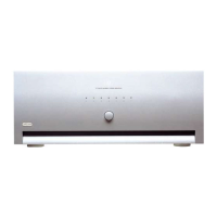
P7 Amplifier Module
Circuit Description
Refer to L924 circuit diagrams
Introduction
L924 is the power amplifier module for the P7 multichannel
amplifier. There are 7 identical modules in the P7. The circuit
design is based on the A85 / A32 output stage topology.
The main features of the amplifier module are as follows:
• Preset ‘THX’ gain (29dB closed loop gain). 0dBV input
signal corresponds to 100 watts into 8Ω output power
• Capable of producing 150 watts of sinusoidal output
power into an 8Ω resistive load (with greater than
250W into 3.2Ω subject to thermal dissipation limits)
• Relay coupled output for silent power on / off and load
protection
• Opto-isolated fault and control lines to the
microprocessor PCB (to avoid hum loops and
instability, to improve EMC performance and crosstalk)
• DC coupled signal path with integrating servo to
remove residual DC errors
• Instantaneous load protection
• Mono block design (each channel is electrically isolated
from all others and has independent power supply
windings on the mains transformer)
• Integrated modular heatsink for good thermal
performance and ease of assembly / servicing
• Low harmonic and intermodulation distortion
• Flat frequency response
• Fast (and symmetrical) slew rate
• High damping factor
• Unconditionally stable into loads of up to ±90° phase
angle
Sheet 1
The input to the amplifier is connected via SK103. The 2
phono sockets are connected in parallel to allow ‘daisy-
chaining’ of amplifier modules. R104 provides a DC leakage
path to the chassis (i.e. mains power earth) to prevent small
transformer leakage currents causing the electrical 0V of the
amplifier to rise significantly above mains earth potential.
C104 provides an EMC coupling between the local input
ground and the chassis to reduce common mode RF noise.
Star point SP101 connects the differently named electrical 0V
nets at a single point. This is to ensure the correct wiring
topology of the ground connections on the printed circuit
board. SP101 provides a good common ground reference
point when making voltage measurements on the PCB. Note
that 0V_DIG is not connected to SP101, as this is the
microprocessor ground.
Relay RLY101 connects the output of the amplifier to the
load via socket SK105.
L101 and R103 form part of a ‘Zobel’ network to decouple
the load at high frequencies to ensure amplifier stability into
capacitive loads.
Note that signals 6 through 9 are open collector outputs,
active low, referred to 0V_DIG with no pull-up resistors.
This is because they are wire OR’d on the microprocessor
PCB (L925), where the pull-up resistors to +5V digital are
located.
The line ‘NFB’ provides for a portion of the negative feedback of the
amplifier to be taken on the load side of RLY101. The components
that allow for this (R236 thru R239) are not presently fitted, meaning
that RLY101 is not included in the feedback loop.
SK104 connects to the microcontroller PCB. Note that all signals on
this connector are electrically isolated from the amplifier circuit
itself, via either opto isolators or the relay coil of RLY101. The 10-
pin connector has the following signals:
SK104
Pin Type Name Description
1 GND 0V DIG Microprocessor ground return
2 PSU +24V_DIG +24 volt digital power supply
(referred to 0V_DIG only) for
relay coil RLY101
3 MUTE Not used
4 I/P OUT_RLY Relay drive for the output relay
RLY101 (LOW = output relay
ON)
5 Not used
6 O/P THERMPR
OT
Open collector thermal fault signal
(LOW = FAULT)
7 O/P VIPROT Open collector short circuit fault
signal (LOW = FAULT)
8 O/P DCPROT Open collector DC fault signal
(LOW = FAULT)
9 O/P FAULT Open collector overall fault signal
(LOW = FAULT)
10 Not used
Sheet 2
Port INPUT connects the input of the amplifier, referred to 0V_SIG,
which is the precision signal ground reference.
Zener diodes DZ202 and DZ203 limit the input signal amplitude to
approximately 5.3Vpk. This is to prevent damage to the input of op-
amp IC200, due to a leaky source signal or electrostatic discharge.
R223, R228 and C210 form a passive 1
st
order low pass filter with a –
3dB corner frequency of roughly 330kHz to prevent ultrasonic
signals from entering the circuit and possibly causing damage.
The main amplifier circuit is a ‘classic’ current feedback design.
IC200A is configured as a non-inverting amplifier with a gain of 2.
Its purpose is to provide current outputs (via its power supply pins)
and a current input (via its output pin). This forms the voltage to
current (transimpedance) conversion and phase splitting necessary to
drive the voltage gain stage. The ‘current feedback’ occurs because
when IC200 drives its 44Ω load to ground, the power supply pin
currents are half-wave rectified versions of the drive current of the
amplifier. This causes voltage gain, which is buffered and passed on
to the outputs. The feedback from the output to pin 1 of IC200 acts to
reduce the gain of the amplifier; when this current is roughly equal to
the current required to drive the input signal into 44Ω, equilibrium is
reached and the closed loop gain is defined. The output stage
provides the vast majority of the current required to drive the 44Ω
signals to ground. The op-amp only provides a very small error
current sufficient to give the required voltage magnification.
Transistors TR204 and TR203 are wired as cascodes (common base
amplifiers). Their purpose is to provide IC200 with ±15V power
supply rails, whilst allowing IC200’s power supply pin currents to
pass through them to the NPN and PNP current mirrors.
The resistor, zener diode and capacitor circuits on the bases of TR204
and TR203 are to provide a controlled ramp up during power on, a
stable power supply voltage and good local HF decoupling.
 Loading...