2122
STICKY Pad Placement:
Now that you made it here safely I hope, go back one step to AC SW
PCB Mounting.
Welcome travelers to my ‘pad’. Please make yourself at home, but first
lets tidy up this place shall we.
q Cable Tie Mount Pad x 1
q 3” Cable Ties x 3
q Remove the paper on the back of the Cable Tie Mount Pad to
expose the sticky surf a c e .
q S q u a re l y, stick this tie mount pad to the chassis directly below
w h e re the wires will be routed. Basically half way along the line fro m
w h e re the wires exit the chassis access hole to the edge of the
chassis. Press it down very firm l y. CUE: Dust the floor of the chassis
in this area first.
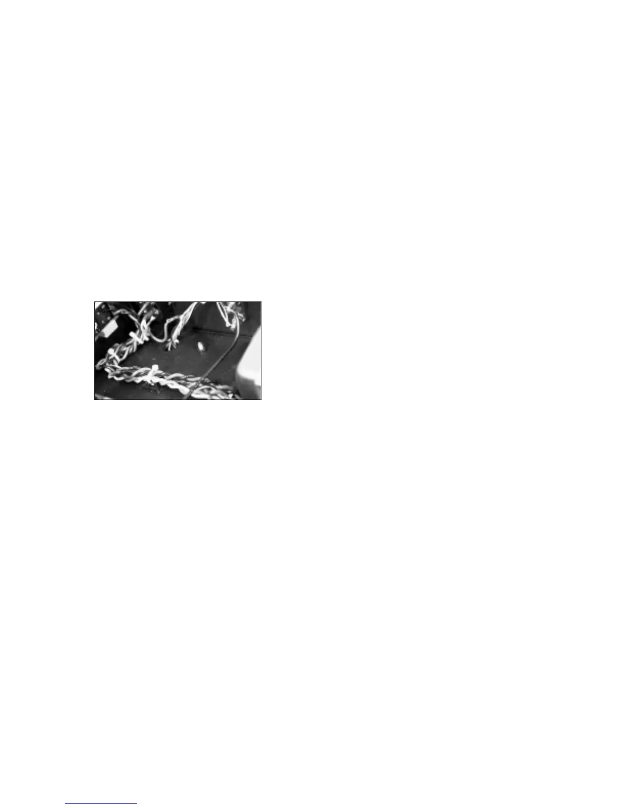
q G roup these wires neatly, tuck them into place in the corners, or
f o rm them as needed to create a duct-work like effect.
q Slide one of the Cable Ties through the Tie Mount Pad channels and
a round the bundle of wires, mate it and tighten it down. Now using two
m o re ties, bundle these wires as you see fit. The photo is a good
guide. CUE: The pair of wires with no home, may be folded back
along with the bundle and wire tied together.
Just a quickie here to change the pace a bit. A Black Nylon plug
needs to be installed into the rear panel hole that is located between
the RCA jacks and the Right Speaker binding posts. It just snaps into
place. This is where you may install the attenuator so that the amp
may be feed directly from your favorite source device.
It is good to see that every one is keeping up with me. Since I am
going to take a break now, may I suggest that if you have not taken a
b reak yet for awhile, this is a good time to do so as well. See you
l a t e r......and don’t re s t a rt without me, I don’t want to miss anything that
you are doing!
Chassis Wiring (Part 3):
Installation of PC Boards:
Get re a d y, we are on the home stretch. In a few moments we will be
p reparing the power transformer secondary winding wires and
installing the remaining PCB’s and their interconnecting power supply
w i res. As usual, this is not difficult when done in an orderly fashion.
Also, when it comes to this part of the construction process of wiring,
it is very important and at times difficult, to keep it neat. As it is my
responsibility to guide you through to a result of a professional looking
a m p l i f i e r, we will apply a few touches of finesse and you may even
end up with a piece of art? Oh boy, there ’s an ego trip. So let’s turn up
the music and do the twist!
q Rev up your drill again and snugly twist all the like coloured Power
Tr a n s f o rmer wire pairs together. The RED with YELLOW stripe wire will
also be twisted with the pair of RED wire s .
q Once twisted, cut the twisted pairs to the following lengths,
m e a s u red from the chassis access hole outward s :
q RED pr. & RED/YEL 7” (178mm)
q YELLOW pr. 6 1/4” (159mm)
q VIOLET pr. 8 (203mm)
q G R AY pr. 9 1/4” (235mm)
q GREEN pr. 7 1/2” (216mm)
q BLUE pr. 11 3/4” (298mm)
P re p a re all of these wire sets for soldering, we will need them soon.
Main Filter Bank Connections:
S t a rting here we will be interconnecting all the remaining PCB’s before
mounting them to the chassis.
q Black 18awg 3 3/4” (95mm) x 1
q Black 18awg 6” (152mm) x 1
q Black 18awg 6 3/4” (170mm) x 1
q Red 18awg 3” (76mm) x 1 (Sig)
q Red 18awg 5” (127mm) x 1 (Sig)
q B rown 18awg 6” (165mm) x 2
q Blue 18awg 5” (127mm) x 2
You have done such a great job in preparing all of these wires! So lets
put them where they belong.
Connecting one wire at a time, start with this one.
q Black 18awg 3 3/4” (95mm) x 1
This wire interconnects the Main Filter Bank power supply common to
the Main PCB common. First we will connect one end of this wire to
the Main Filter Bank PCB to the pad labeled ‘COM’ which is indicated
by the line pointing to the center pad in the common cluster (4 pads
consisting of Com, C/T, L, R. CUE: add a few vowels). Connect this
w i re from underneath the PCB. The opposite end will be connected
s o o n .
Locate these wire s :
q Black 18awg 6” (152mm) x 1
q Red 18awg 5” (127mm) x 1 (Sig)
q Still on the Main Filter Bank PCB connect the above Black wire to
the pad labeled ‘L’ in the common cluster.
q Then connect the above RED wire to the pad labeled ‘LB+1’. Tr i m
the soldered leads.
Moving on to the Right channel H. V. connections we do the same
thing. Locate these wire s .
q Black 18awg 6 3/4” (170mm) x 1
q Red 18awg 3” (76mm) x 1 (Sig)
q Again, from the bottom side on the Main Filter Bank PCB connect
the above Black wire this time to the pad labeled ‘R’ in the common
c l u s t e r.
q Then connect the above RED wire to the pad labeled ‘B+1’.
Remember to trim the soldered leads.
Left and Right Filter Bank Connections:
Each channel has its own separate input/driver stage power supply
filtering, a dual mono arrangement. This approach helps to furt h e r
isolate the most sensitive gain stages. Gather up the Left Filter Bank
and the Right Filter Bank PC boards. Next we will connect the B+
w i res that will connect to the Main PCB and then complete the
connections to the Main Filter Bank.
q Main Filter PCB x 1
q Left Filter Bank PCB x 1
q Right Filter Bank PCB x 1
q B rown 18awg 6” (165mm) x 2
q Blue 18awg 5” (127mm) x 2
As before, or shall I say, to conform to our style these wires are
connected from underneath the PCB’s.
q Connect the two Brown wires to the B+2 and LB+2 pad locations on
the Right and Left Filter Banks.
q Then do the same with the Blue wires connecting them to the B+3
and LB+3 pads on both boards. Trim the excess wire leads above the
b o a rd s .
Now complete the connections to the Main Filter Bank - connecting
the wiring from the Left and Right Filter Banks to the Main Filter
Bank. You will see the obvious wire connections to be made, which
are;
 Loading...