Hardware Description
2-5 AT89STK-11 Hardware User Guide
7676B–8051–08/07
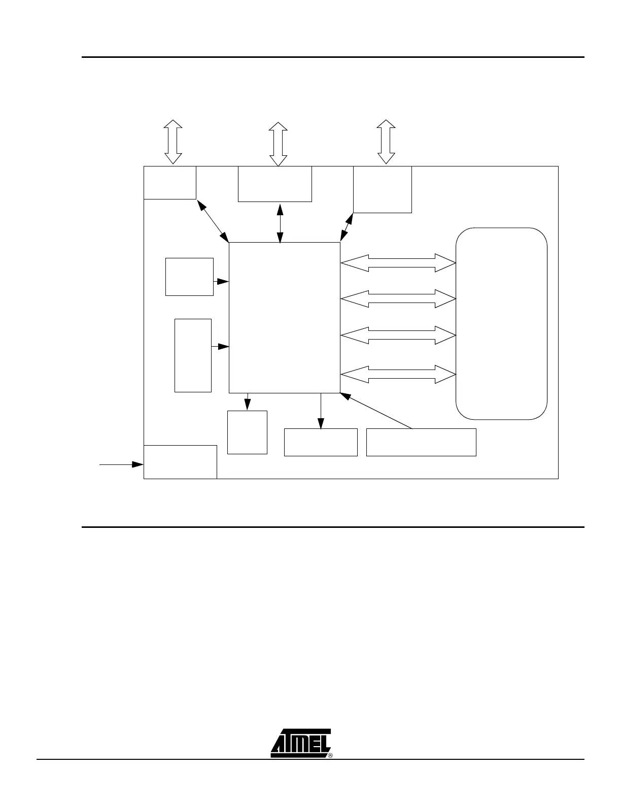
2.2 Block Diagram
Figure 2-2 shows the functional block diagram of the AT89STK-11, with the I/O usage.
Figure 2-2. Block Diagram of AT89STK-11
2.3 Power Supply
The on-board power supply circuitry allows various power supply configurations. This
gives the user the capability to power the devices in the 3V and in the 5V voltage range.
2.3.1 Power Supply
Sources
The power supply source can come from two different and exclusive sources:
either from the JACK PWR connector
either from the 2-point sip EXT connector.
2.3.1.1 JACK PWR
Connector
The Jack power connector implemented on board is a female Jack connector with inter-
nal 2.1mm conductor. It requires a male JACK outlet with 2.1mm capability.
No specific polarization is mandatory as on-board diode rectifier gives a protection
against inadvertent polarization invertion.
When using the JACK power supply, the board is powered with a 5V voltage.
Power Supply
Full UART
External
Power
PC Host
C51
P2
P3
EA
RST
ISP
Expansion
TWI
P0
P1
SPI
INT0
Leds:
PWR
ALE
16MHz
Quartz
PLCC44
3V or 5V
INT1
Area
User LEDs User Push Buttons
 Loading...