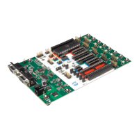
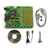
Hardware Description
AT89STK-11 Hardware User Guide 2-8
7676B–8051–08/07
This interface enables the debug of the application through ATMEL OCD dongle for
AT89C51RE2/IE2/RD3/IE3 only.
2.6.5 Expansion Area In addition to a 16x29 pad array, two rows of pads are given on the right side of the
board to offer all the MCU signals tu user application. Any application expansion can be
built on board through this interface.
2.7 Board Settings
The C51 Demo Board has the following settings:
Jumpers
Solder straps
Test points
2.7.1 Jumpers The following table provides an overview of the jumpers, the solder straps and their
default configuration.
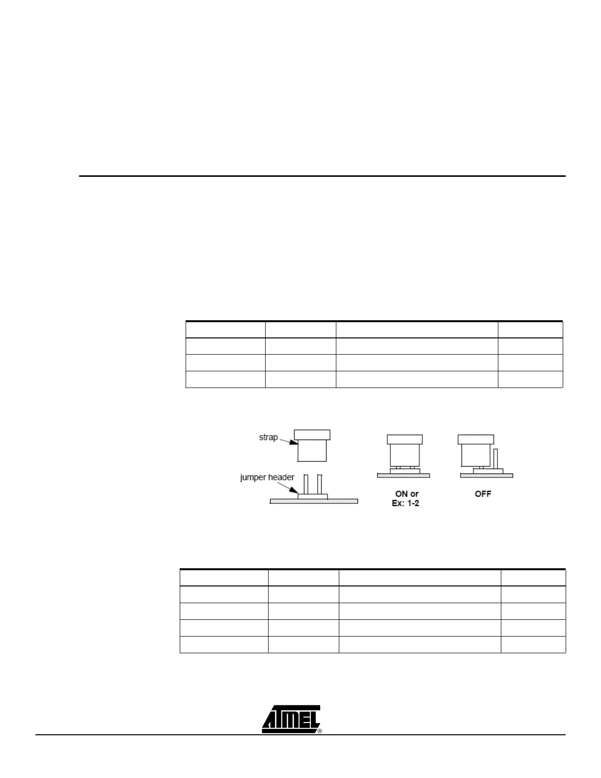
Figure 2-5. Jumper Setting Definition
2.7.2 Solder Straps Solder straps allow to modify the board configuration for specific usage.
Table 2-1. Jumpers and Switches Overview
Reference PCB Label Function Default
Jumper J11 J11 RTS of RS232 OFF
Jumper J12 J12 DTR of RS232 OFF
Jumper J13 J13 OFF
Table 2-2. Solder Straps Overview
Reference PCB Label Function Default
Solder strap SP1 SP1 External Power Supply Isolation Soldered
Solder strap SP2 ICC Consumption measurement Soldered
Solder strap SP3 SP3 Rx Led Soldered
Solder strap SP4 SP4 Tx Led Soldered
 Loading...