207
8271D–AVR–05/11
ATmega48A/PA/88A/PA/168A/PA/328/P
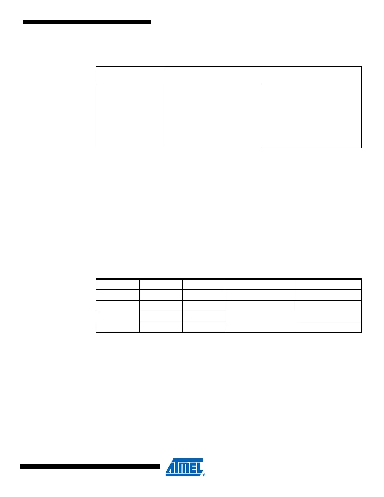
Note: 1. The baud rate is defined to be the transfer rate in bit per second (bps)
BAUD Baud rate (in bits per second, bps)
f
OSC
System Oscillator clock frequency
UBRRn Contents of the UBRRnH and UBRRnL Registers, (0-4095)
21.4 SPI Data Modes and Timing
There are four combinations of XCKn (SCK) phase and polarity with respect to serial data, which
are determined by control bits UCPHAn and UCPOLn. The data transfer timing diagrams are
shown in Figure 21-1. Data bits are shifted out and latched in on opposite edges of the XCKn
signal, ensuring sufficient time for data signals to stabilize. The UCPOLn and UCPHAn function-
ality is summarized in Table 21-2. Note that changing the setting of any of these bits will corrupt
all ongoing communication for both the Receiver and Transmitter.
Table 21-1. Equations for Calculating Baud Rate Register Setting
Operating Mode
Equation for Calculating Baud
Rate
(1)
Equation for Calculating UBRRn
Value
Synchronous Master
mode
BAUD
f
OSC
2 UBRRn 1+()
---------------------------------------=
UBRRn
f
OSC
2BAUD
-------------------- 1–=
Table 21-2. UCPOLn and UCPHAn Functionality-
UCPOLn UCPHAn SPI Mode Leading Edge Trailing Edge
0 0 0 Sample (Rising) Setup (Falling)
0 1 1 Setup (Rising) Sample (Falling)
1 0 2 Sample (Falling) Setup (Rising)
1 1 3 Setup (Falling) Sample (Rising)