249
8271D–AVR–05/11
ATmega48A/PA/88A/PA/168A/PA/328/P
.
23.3 Register Description
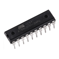
23.3.1 ADCSRB – ADC Control and Status Register B
• Bit 6 – ACME: Analog Comparator Multiplexer Enable
When this bit is written logic one and the ADC is switched off (ADEN in ADCSRA is zero), the
ADC multiplexer selects the negative input to the Analog Comparator. When this bit is written
logic zero, AIN1 is applied to the negative input of the Analog Comparator. For a detailed
description of this bit, see ”Analog Comparator Multiplexed Input” on page 248.
23.3.2 ACSR – Analog Comparator Control and Status Register
• Bit 7 – ACD: Analog Comparator Disable
When this bit is written logic one, the power to the Analog Comparator is switched off. This bit
can be set at any time to turn off the Analog Comparator. This will reduce power consumption in
Active and Idle mode. When changing the ACD bit, the Analog Comparator Interrupt must be
disabled by clearing the ACIE bit in ACSR. Otherwise an interrupt can occur when the bit is
changed.
• Bit 6 – ACBG: Analog Comparator Bandgap Select
When this bit is set, a fixed bandgap reference voltage replaces the positive input to the Analog
Comparator. When this bit is cleared, AIN0 is applied to the positive input of the Analog Compar-
ator. When the bandgap reference is used as input to the Analog Comparator, it will take a
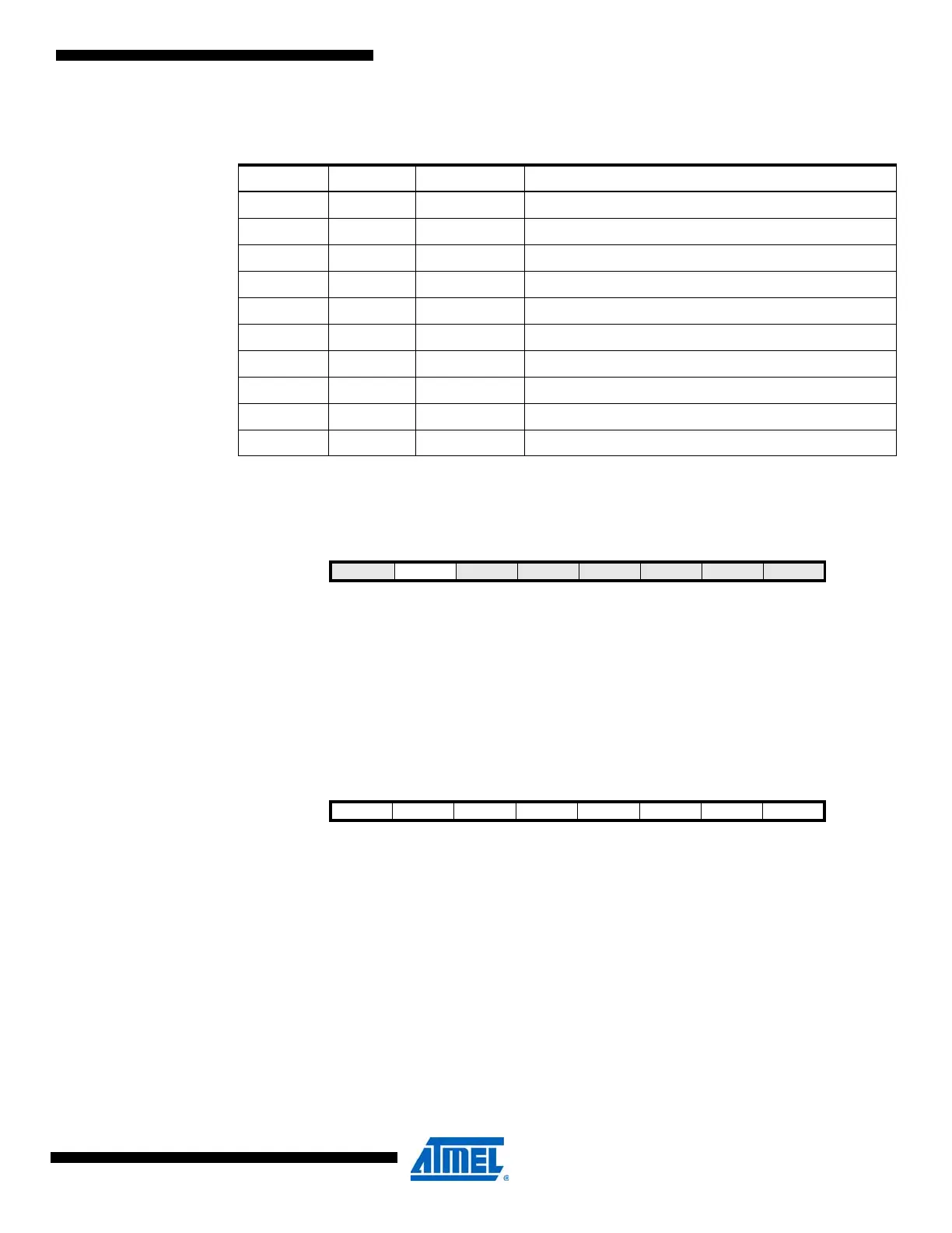
Table 23-1. Analog Comparator Multiplexed Input
ACME ADEN MUX2...0 Analog Comparator Negative Input
0 x xxx AIN1
1 1 xxx AIN1
1 0 000 ADC0
1 0 001 ADC1
1 0 010 ADC2
1 0 011 ADC3
1 0 100 ADC4
1 0 101 ADC5
1 0 110 ADC6
1 0 111 ADC7
Bit 7 6543210
(0x7B)
–ACME– – – ADTS2 ADTS1 ADTS0 ADCSRB
Read/Write R R/W R R R R/W R/W R/W
Initial Value0 0000000
Bit 76543210
0x30 (0x50) ACD ACBG ACO ACI ACIE ACIC ACIS1 ACIS0 ACSR
Read/Write R/W R/W R R/W R/W R/W R/W R/W
Initial Value 0 0 N/A 0 0 0 0 0