304
8271D–AVR–05/11
ATmega48A/PA/88A/PA/168A/PA/328/P
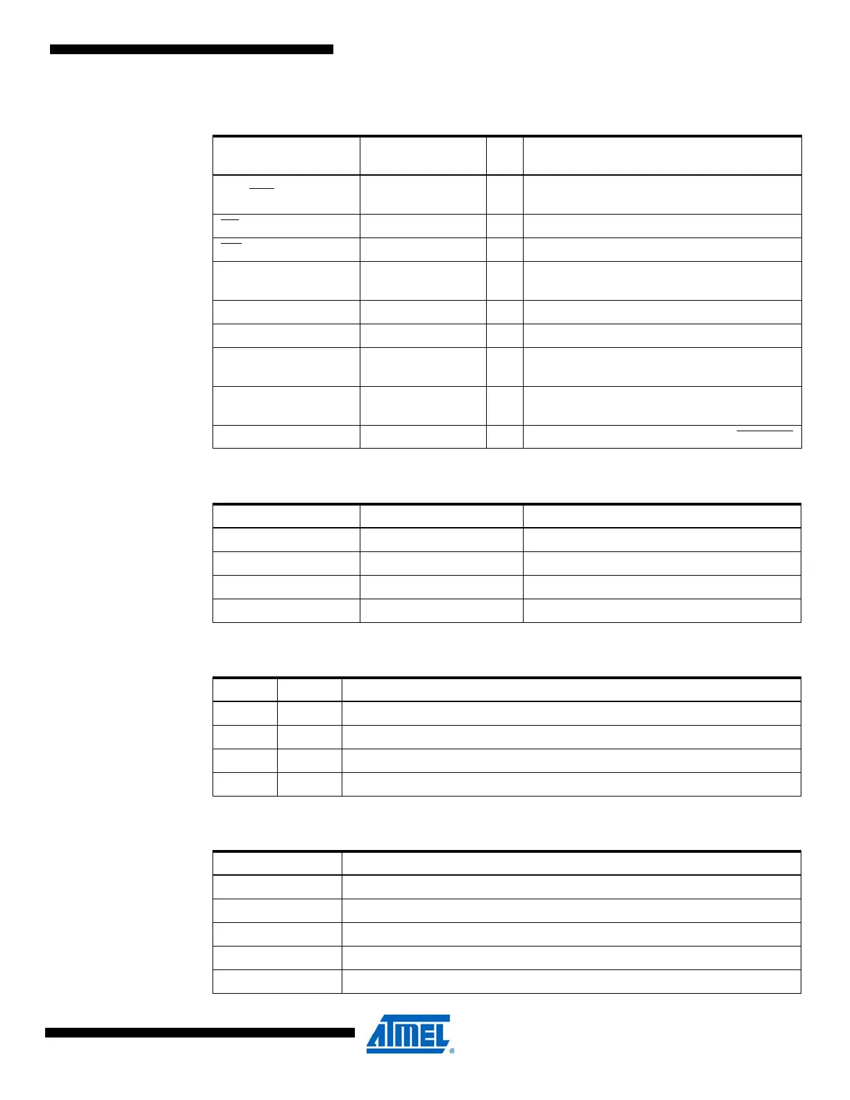
Table 28-13. Pin Name Mapping
Signal Name in
Programming Mode Pin Name I/O Function
RDY/BSY PD1 O
0: Device is busy programming, 1: Device is
ready for new command
OE
PD2 I Output Enable (Active low)
WR
PD3 I Write Pulse (Active low)
BS1 PD4 I
Byte Select 1 (“0” selects Low byte, “1” selects
High byte)
XA0 PD5 I XTAL Action Bit 0
XA1 PD6 I XTAL Action Bit 1
PAG E L PD7 I
Program memory and EEPROM Data Page
Load
BS2 PC2 I
Byte Select 2 (“0” selects Low byte, “1” selects
2’nd High byte)
DATA {PC[1:0]: PB[5:0]} I/O Bi-directional Data bus (Output when OE is low)
Table 28-14. Pin Values Used to Enter Programming Mode
Pin Symbol Value
PAGEL Prog_enable[3] 0
XA1 Prog_enable[2] 0
XA0 Prog_enable[1] 0
BS1 Prog_enable[0] 0
Table 28-15. XA1 and XA0 Coding
XA1 XA0 Action when XTAL1 is Pulsed
0 0 Load Flash or EEPROM Address (High or low address byte determined by BS1).
0 1 Load Data (High or Low data byte for Flash determined by BS1).
1 0 Load Command
1 1 No Action, Idle
Table 28-16. Command Byte Bit Coding
Command Byte Command Executed
1000 0000 Chip Erase
0100 0000 Write Fuse bits
0010 0000 Write Lock bits
0001 0000 Write Flash
0001 0001 Write EEPROM