303
8271D–AVR–05/11
ATmega48A/PA/88A/PA/168A/PA/328/P
28.6 Parallel Programming Parameters, Pin Mapping, and Commands
This section describes how to parallel program and verify Flash Program memory, EEPROM
Data memory, Memory Lock bits, and Fuse bits in the ATmega48A/PA/88A/PA/168A/PA/328/P.
Pulses are assumed to be at least 250 ns unless otherwise noted.
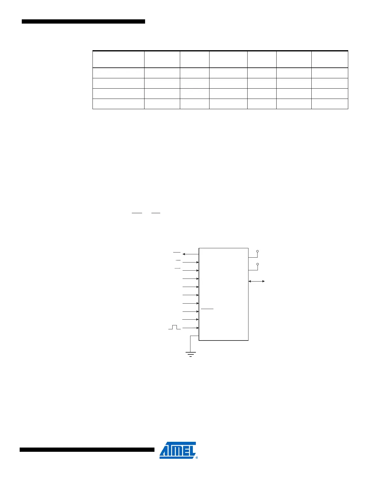
28.6.1 Signal Names
In this section, some pins of the ATmega48A/PA/88A/PA/168A/PA/328/P are referenced by sig-
nal names describing their functionality during parallel programming, see Figure 28-1 and Table
28-13. Pins not described in the following table are referenced by pin names.
The XA1/XA0 pins determine the action executed when the XTAL1 pin is given a positive pulse.
The bit coding is shown in Table 28-15.
When pulsing WR
or OE, the command loaded determines the action executed. The different
Commands are shown in Table 28-16.
Figure 28-1. Parallel Programming
Note: V
CC
- 0.3V < AV
CC
< V
CC
+ 0.3V, however, AV
CC
should always be within 4.5 - 5.5V
ATmega168A 512bytes 4bytes EEA[1:0] 128 EEA[8:2] 8
ATmega168PA 512bytes 4bytes EEA[1:0] 128 EEA[8:2] 8
ATmega328 1Kbytes 4bytes EEA[1:0] 256 EEA[9:2] 9
ATmega328P 1Kbytes 4bytes EEA[1:0] 256 EEA[9:2] 9
Table 28-12. No. of Words in a Page and No. of Pages in the EEPROM
Device
EEPROM
Size
Page
Size PCWORD
No. of
Pages PCPAGE EEAMSB
VCC
GND
XTAL1
PD1
PD2
PD3
PD4
PD5
PD6
PC[1:0]:PB[5:0]
DATA
RESET
PD7
+12 V
BS1
XA0
XA1
OE
RDY/BSY
PAGEL
PC2
WR
BS2
AVCC
+4.5 - 5.5V
+4.5 - 5.5V