124
7598H–AVR–07/09
ATtiny25/45/85
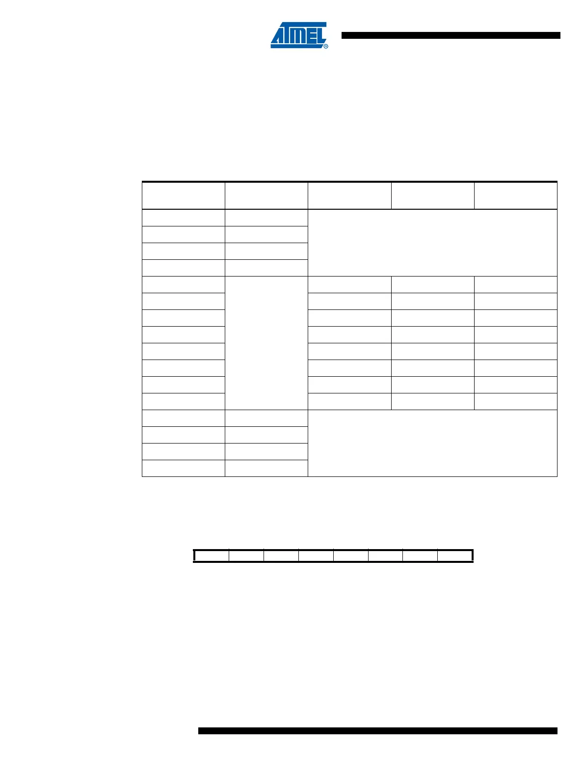
• Bits 3:0 – MUX3:0: Analog Channel and Gain Selection Bits
The value of these bits selects which combination of analog inputs are connected to the ADC. In
case of differential input (ADC0 - ADC1 or ADC2 - ADC3), gain selection is also made with these
bits. Selecting ADC2 or ADC0 as both inputs to the differential gain stage enables offset mea-
surements. Selecting the single-ended channel ADC4 enables the temperature sensor. Refer to
Table 18-4 for details. If these bits are changed during a conversion, the change will not go into
effect until this conversion is complete (ADIF in ADCSRA is set).
18.7.6 ADC Control and Status Register A – ADCSRA
• Bit 7 – ADEN: ADC Enable
Writing this bit to one enables the ADC. By writing it to zero, the ADC is turned off. Turning the
ADC off while a conversion is in progress, will terminate this conversion.
• Bit 6 – ADSC: ADC Start Conversion
In Single Conversion mode, write this bit to one to start each conversion. In Free Running mode,
write this bit to one to start the first conversion.
Table 18-4. Input Channel Selections
MUX3..0
Single Ended
Input
Positive
Differential Input
Negative
Differential Input Gain
0000 ADC0 (PB5)
N/A
0001 ADC1 (PB2)
0010 ADC2 (PB4)
0011 ADC3 (PB3)
0100
N/A
ADC2 (PB3) ADC2 (PB3) 1x
0101
(1)
1. For offset calibration only . See “Operation” on page 112.
ADC2 (PB3) ADC2 (PB3) 20x
0110 ADC2 (PB3) ADC3 (PB4) 1x
0111 ADC2 (PB3) ADC3 (PB4) 20x
1000 ADC0 (PB5) ADC0 (PB5) 1x
1001 ADC0 (PB5) ADC0 (PB5) 20x
1010 ADC0 (PB5) ADC1 (PB2) 1x
1011 ADC0 (PB5) ADC1 (PB2) 20x
1100 1.1V/2.56V
N/A
1101 0V
1110 N/A
1111 ADC4
(2)
2. For Temperature Sensor
Bit 76543210
ADEN ADSC ADATE ADIF ADIE ADPS2 ADPS1 ADPS0 ADCSRA
Read/Write R/W R/W R/W R/W R/W R/W R/W R/W
Initial Value 0 0 0 0 0 0 0 0