17
AT90S/LS2323/2343
1004D–09/01
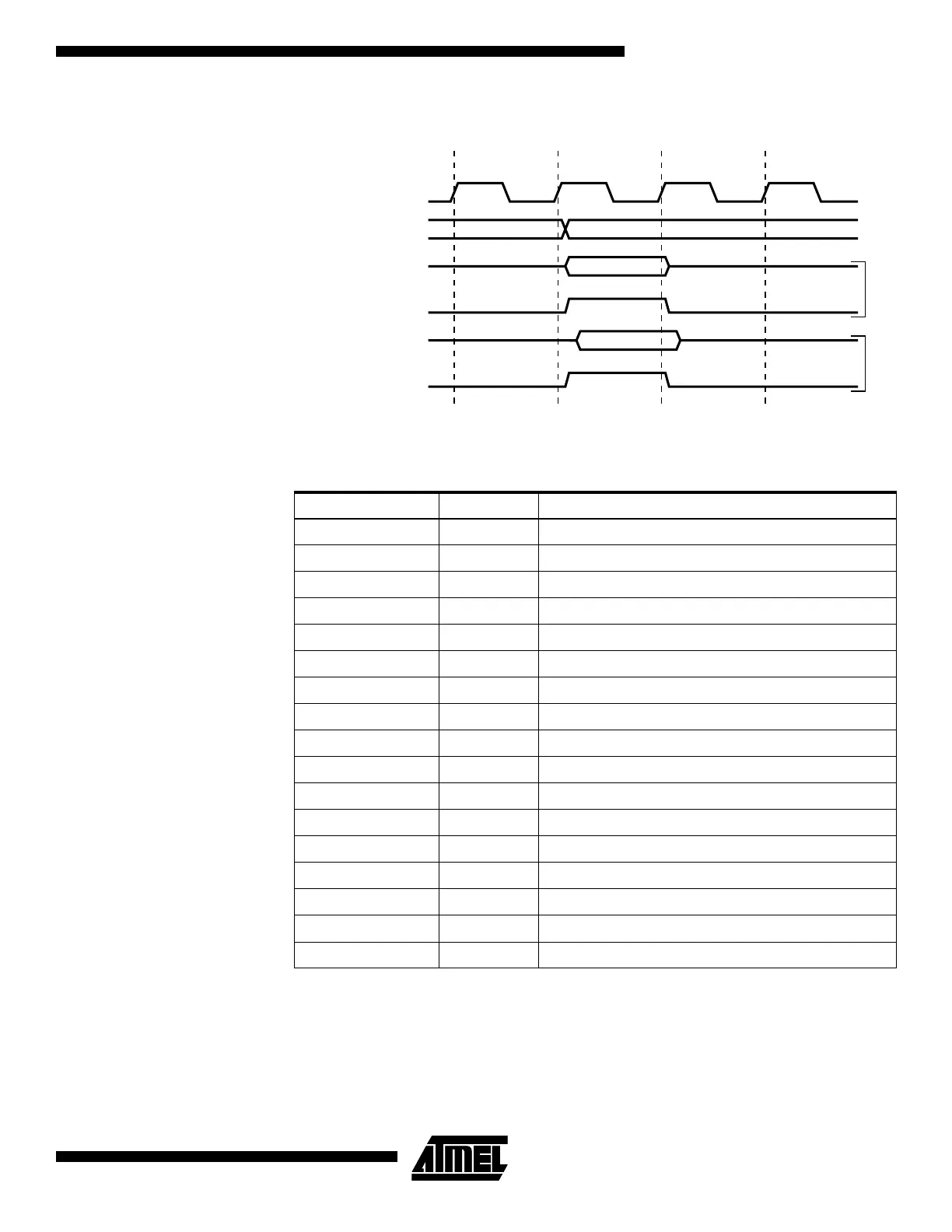
Figure 23. On-chip Data SRAM Access Cycles
I/O Memory The I/O space definition of the AT90S2323/2343 is shown in Table 2.
Note: Reserved and unused locations are not shown in the table.
All AT90S2323/2343 I/Os and peripherals are placed in the I/O space. The I/O locations
are accessed by the IN and OUT instructions transferring data between the 32 general-
purpose working registers and the I/O space. I/O registers within the address range $00
- $1F are directly bit-accessible using the SBI and CBI instructions. In these registers,
the value of single bits can be checked by using the SBIS and SBIC instructions. Refer
to the instruction set section for more details. When using the I/O-specific commands IN
System Clock Ø
WR
RD
Data
Data
Address
Address
T1 T2 T3 T4
Prev. Address
Read
Write
Table 2. AT90S2323/2343 I/O Space
Address Hex Name Function
$3F ($5F) SREG Status REGister
$3D ($5D) SPL Stack Pointer Low
$3B ($5B) GIMSK General Interrupt MaSK register
$3A ($5A) GIFR General Interrupt Flag Register
$39 ($59) TIMSK Timer/Counter Interrupt MaSK register
$38 ($58) TIFR Timer/Counter Interrupt Flag register
$35 ($55) MCUCR MCU Control Register
$34 ($54) MCUSR MCU Status Register
$33 ($53) TCCR0 Timer/Counter0 Control Register
$32 ($52) TCNT0 Timer/Counter0 (8-bit)
$21 ($41) WDTCR Watchdog Timer Control Register
$1E ($3E) EEAR EEPROM Address Register
$1D ($3D) EEDR EEPROM Data Register
$1C ($3C) EECR EEPROM Control Register
$18 ($38) PORTB Data Register, Port B
$17 ($37) DDRB Data Direction Register, Port B
$16 ($36) PINB Input Pins, Port B

 Loading...


