10
AT90S/LS2323/2343
1004D–09/01
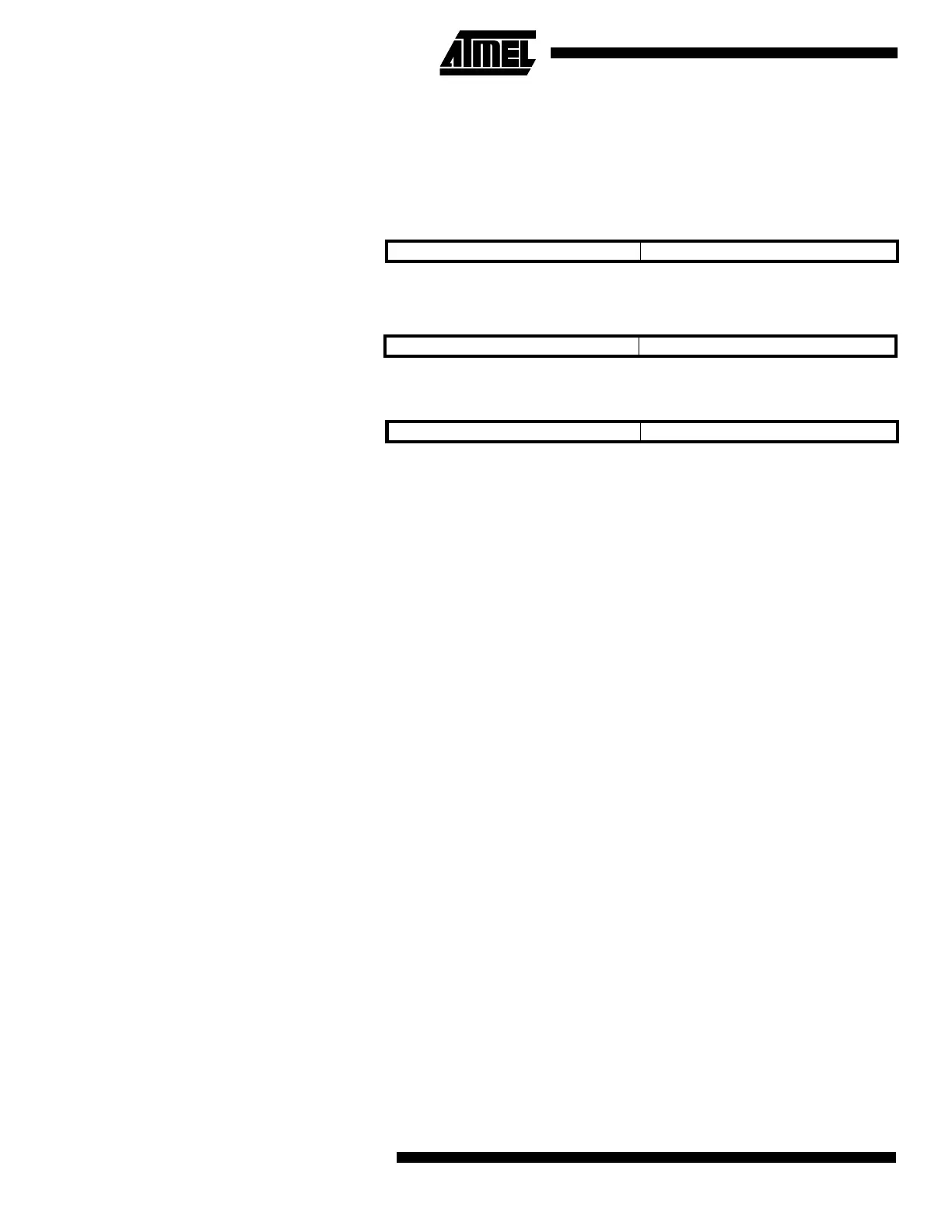
X-register, Y-register and Z-
register
The registers R26..R31 have some added functions to their general-purpose usage.
These registers are the address pointers for indirect addressing of the Data Space. The
three indirect address registers X, Y, and Z, are defined in Figure 8.
Figure 8. The X-, Y-, and Z-registers
In the different addressing modes, these address registers have functions as fixed dis-
placement, automatic increment and decrement (see the descriptions for the different
instructions).
ALU – Arithmetic Logic
Unit
The high-performance AVR ALU operates in direct connection with all the 32 general-
purpose working registers. Within a single clock cycle, ALU operations between regis-
ters in the register file are executed. The ALU operations are divided into three main
categories: arithmetic, logic and bit functions.
In-System
Programmable Flash
Program Memory
The AT90S2323/2343 contains 2K bytes On-chip, In-System Programmable Flash
memory for program storage. Since all instructions are 16- or 32-bit words, the Flash is
organized as 1K x 16. The Flash memory has an endurance of at least 1000 write/erase
cycles.
The AT90S2323/2343 Program Counter (PC) is 10 bits wide, hence addressing the
1024 program memory addresses. See page 42 for a detailed description on Flash data
programming.
Constant tables must be allocated within the address 0 - 2K (see the LPM – Load Pro-
gram Memory instruction description on page 60).
See page 12 for the different addressing modes.
EEPROM Data Memory The AT90S2323/2343 contains 128 bytes of EEPROM data memory. It is organized as
a separate data space, in which single bytes can be read and written. The EEPROM has
an endurance of at least 100,000 write/erase cycles. The access between the EEPROM
and the CPU is described on page 32, specifying the EEPROM address register, the
EEPROM data register and the EEPROM control register.
For the SPI data downloading, see page 42 for a detailed description.
15 0
X-register 7 0 7 0
R27 ($1B) R26 ($1A)
15 0
Y-register 7 0 7 0
R29 ($1D) R28 ($1C)
15 0
Z-register 7 0 7 0
R31 ($1F) R30 ($1E)

 Loading...


