EasyManua.ls Logo

Atmel AVR AT90S2323 User Manual

Atmel AVR AT90S2323
64 pages
To Next Page IconTo Next Page
To Previous Page IconTo Previous Page
Page #2 background image
2
AT90S/LS2323/2343
1004D09/01
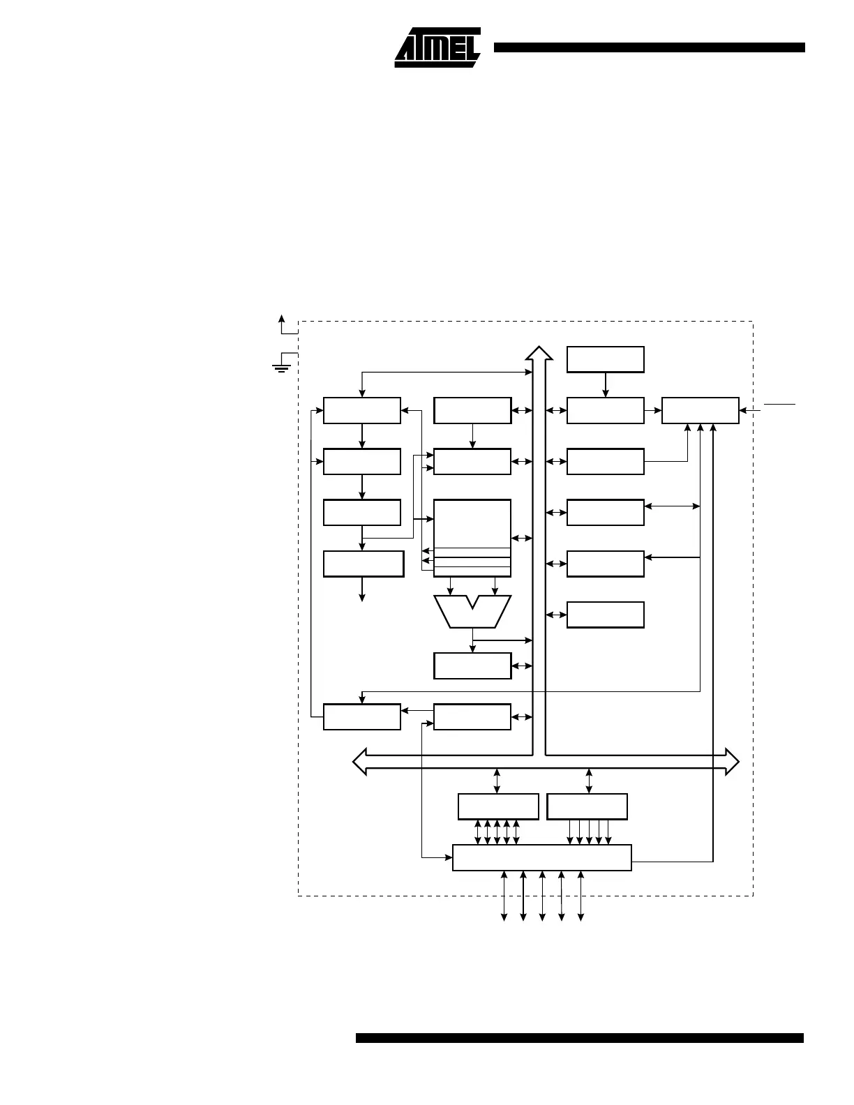
Description The AT90S/LS2323 and AT90S/LS2343 are low-power, CMOS, 8-bit microcontrollers
based on the AVR RISC architecture. By executing powerful instructions in a single
clock cycle, the AT90S2323/2343 achieves throughputs approaching 1 MIPS per MHz
allowing the system designer to optimize power consumption versus processing speed.
The AVR core combines a rich instruction set with 32 general-purpose working regis-
ters. All the 32 registers are directly connected to the Arithmetic Logic Unit (ALU),
allowing two independent registers to be accessed in one single instruction executed in
one clock cycle. The resulting architecture is more code efficient while achieving
throughputs up to ten times faster than conventional CISC microcontrollers.
Block Diagram Figure 1. The AT90S/LS2343 Block Diagram
PROGRAM
COUNTER
INTERNAL
OSCILLATOR
WATCHDOG
TIMER
STACK
POINTER
PROGRAM
FLASH
MCU CONTROL
REGISTER
SRAM
GENERAL
PURPOSE
REGISTERS
INSTRUCTION
REGISTER
TIMER/
COUNTER
INSTRUCTION
DECODER
DATA DIR.
REG. PORTB
DATA REGISTER
PORTB
PROGRAMMING
LOGIC
TIMING AND
CONTROL
INTERRUPT
UNIT
EEPROM
SPI
STATUS
REGISTER
Z
Y
X
ALU
PORTB DRIVERS
PB0 - PB4
RESET
VCC
GND
CONTROL
LINES
8-BIT DATA BUS

Table of Contents

Question and Answer IconNeed help?

Do you have a question about the Atmel AVR AT90S2323 and is the answer not in the manual?

Atmel AVR AT90S2323 Specifications

General IconGeneral
Architecture8-bit AVR
Flash Memory2 KB
SRAM128 Bytes
EEPROM128 Bytes
ADC Channels0
Timers1 x 8-bit
PWM Channels0
Operating Voltage2.7V to 6V

Summary

Pin Configuration

Clock Options

Crystal Oscillator

Use for external quartz crystal or ceramic resonator.

External Clock

Connect to XTAL1/PB3 for clock input.

Architectural Overview

General-purpose Register File

Memory Components

X, Y, and Z Registers

Address pointers for indirect data addressing.

In-System Programmable Flash

2K bytes for program storage.

EEPROM Data Memory

128 bytes for non-volatile data.

Program and Data Addressing Modes

Register Direct, Single Register Rd

Operand in register d (Rd).

Register Direct, Two Registers Rd and Rr

Operands in Rd and Rr, result in Rd.

I/O and Data Addressing Modes

I/O Direct

Operand address in 6 bits of instruction word.

Data Direct

16-bit data address in LSBs of 2-word instruction.

Data Indirect with Displacement

Address from Y/Z register plus displacement.

Reset and Interrupt Handling

Stack Pointer – SPL

Manages subroutine and interrupt stacks.

Reset Sources

Power-on, external, and watchdog reset types.

Sleep Modes

Idle Mode

Stops CPU, allows peripherals to run.

Power-down Mode

Stops oscillator, minimizes power consumption.

Timer/Counter Functionality

8-bit Timer/Counter0

Counts clock pulses or external events.

EEPROM Read/Write Access

EEPROM Address Register – EEAR

Specifies EEPROM address.

EEPROM Data Register – EEDR

Holds EEPROM data for read/write.

Prevent EEPROM Corruption

I/O Port B Overview

Alternate Functions of Port B

Describes CLOCK, SCK, MISO, MOSI functions.

Memory Programming

Fuse Bits in AT90S/LS2323

SPIEN, FSTRT bits.

Fuse Bits in AT90S/LS2343

SPIEN, RCEN bits.

Electrical Characteristics

Absolute Maximum Ratings

Stress limits for device operation.

DC Characteristics

Electrical parameters vs. voltage/temperature.

Instruction Set Summary

Packaging Information

8P3 PDIP Package

Dimensions for PDIP package.

8S2 SOIC Package

Dimensions for SOIC package.

Related product manuals