ATtiny10/11/12
9
General-purpose Register File
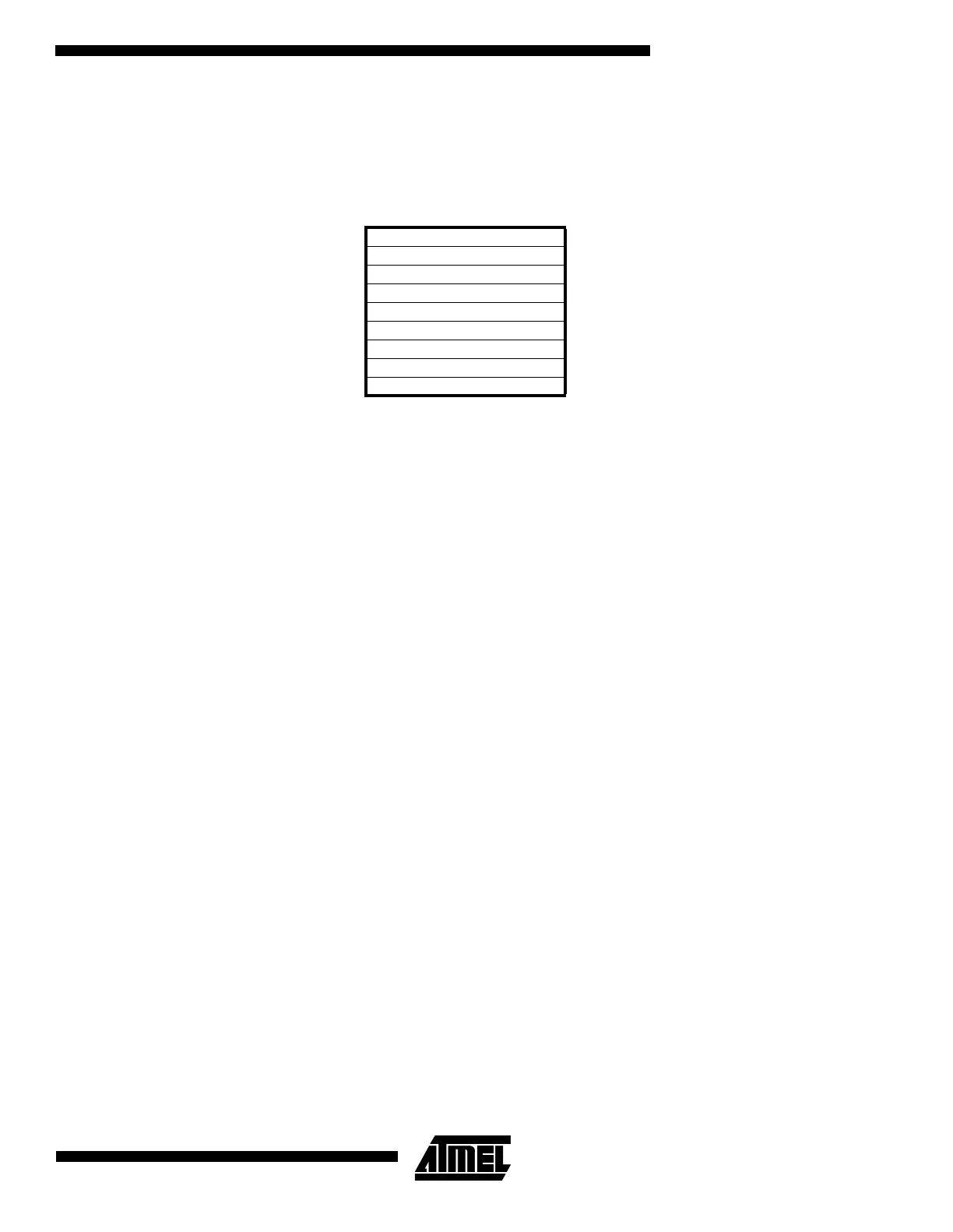
Figure 7 shows the structure of the 32 general-purpose registers in the CPU.
Figure 7. AVR
CPU General-purpose Working Registers
All the register operating instructions in the instruction set have direct- and single-cycle access to all registers. The only
exception is the five constant arithmetic and logic instructions SBCI, SUBI, CPI, ANDI, and ORI between a constant and a
register and the LDI instruction for load-immediate constant data. These instructions apply to the second half of the regis-
ters in the register file – R16..R31. The general SBC, SUB, CP, AND, OR and all other operations between two registers or
on a single register apply to the entire register file.
Registers 30 and 31 form a 16-bit pointer (the Z-pointer) which is used for indirect Flash memory and register file access.
When the register file is accessed, the contents of R31 are discarded by the CPU.
ALU – Arithmetic Logic Unit
The high-performance AVR ALU operates in direct connection with all the 32 general-purpose working registers. Within a
single clock cycle, ALU operations between registers in the register file are executed. The ALU operations are divided into
three main categories – arithmetic, logic and bit-functions. Some microcontrollers in the AVR product family feature a hard-
ware multiplier in the arithmetic part of the ALU.
Flash Program Memory
The ATtiny10/11/12 contains 1K bytes on-chip Flash memory for program storage. Since all instructions are single 16-bit
words, the Flash is organized as 512 x 16 words. The Flash memory has an endurance of at least 1000 write/erase cycles.
The ATtiny10/11/12 Program Counter is 9 bits wide, thus addressing the 512 words Flash program memory.
See page 39 for a detailed description on Flash memory programming.
Program and Data Addressing Modes
The ATtiny10/11/12 AVR RISC Microcontroller supports powerful and efficient addressing modes. This section describes
the different addressing modes supported in the ATtiny10/11/12. In the figures, OP means the operation code part of the
instruction word. To simplify, not all figures show the exact location of the addressing bits.
70
R0
R1
R2
General- …
purpose …
Working R28
Registers R29
R30 (Z-register low byte)
R31 (Z-register high byte)
 Loading...


