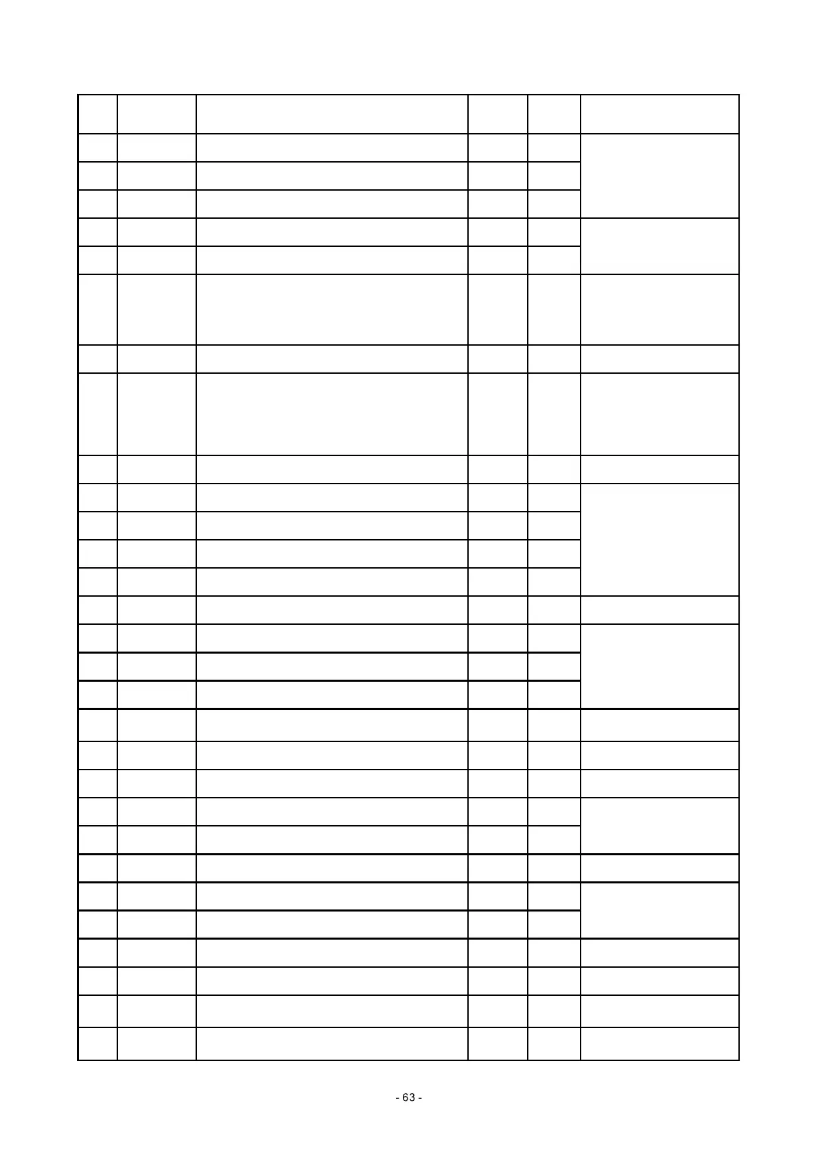
Pin Name Function
Data
direction
DC
voltage
Remark
72 HIGHA3 Microcontroller address bit 3 O 1.11
73 DVDD3 Digital 3.3V power supply 3.24
74 HIGHA2 Microcontroller address bit 2 O 1.81
75 HIGHA1 Microcontroller address bit 1 O 1.55
76 IOA20 Microcontroller address bit 20 O 0
77 IOCS FLASH chip selection O 0
Output PCE# signal and
change into DCE# signal to
control FLASH through 0
ohm resistor R298
78 IOA1 Microcontroller address bit 1 O 2.03 FLASH address signal
79 IOOE FLASH output enable O 0
Output PRD# signal and
change into DRD# signal to
control FLASH output
through 0 ohm resistor
R299
80 DVDD3 Power supply 3.23
81 AD0 Microcontroller address/data bit 0 I/O 1.32
82 AD1 Microcontroller address/data bit 1 I/O 1.52
83 AD2 Microcontroller address/data bit 2 I/O 1.16
84 AD3 Microcontroller address/data bit 3 I/O 0.9
85 DVSS Ground 0
86 AD4 Microcontroller address/data bit 4 I/O 1.57
87 AD5 Microcontroller address/data bit 5 I/O 1.57
88 AD6 Microcontroller address/data bit 6 I/O 1.57
89 IOA21/ADIN0 Microcontroller address bit 21/AD universal input O 0.03 FLASH address signal
90 ALE Microcontroller address enable O 1.18 unused
91 AD7 Microcontroller address/data bit 7 I/O 1.6 FLASH data signal
92 A17 FLASH address bit 17 O 0
93 IOA0 Microcontroller address bit 0 O 2.04
94 DVSS Digital 0
95 UWR Microcontroller write operation 3.22
96 URD Microcontroller read operation 3.26
97 DVDD18 Digital 1.8V power supply 1.92
98 UP1_2 Microcontroller port 0 unused
99 UP1_3 Microcontroller port O 5.15
Panel communication-used
clock
100 UP1_4 Microcontroller port I/O 5.2
Panel communication-used
data
FLASH address signal
FLASH address signal
unused
FLASH data signal
FLASH data signal
FLASH address signal