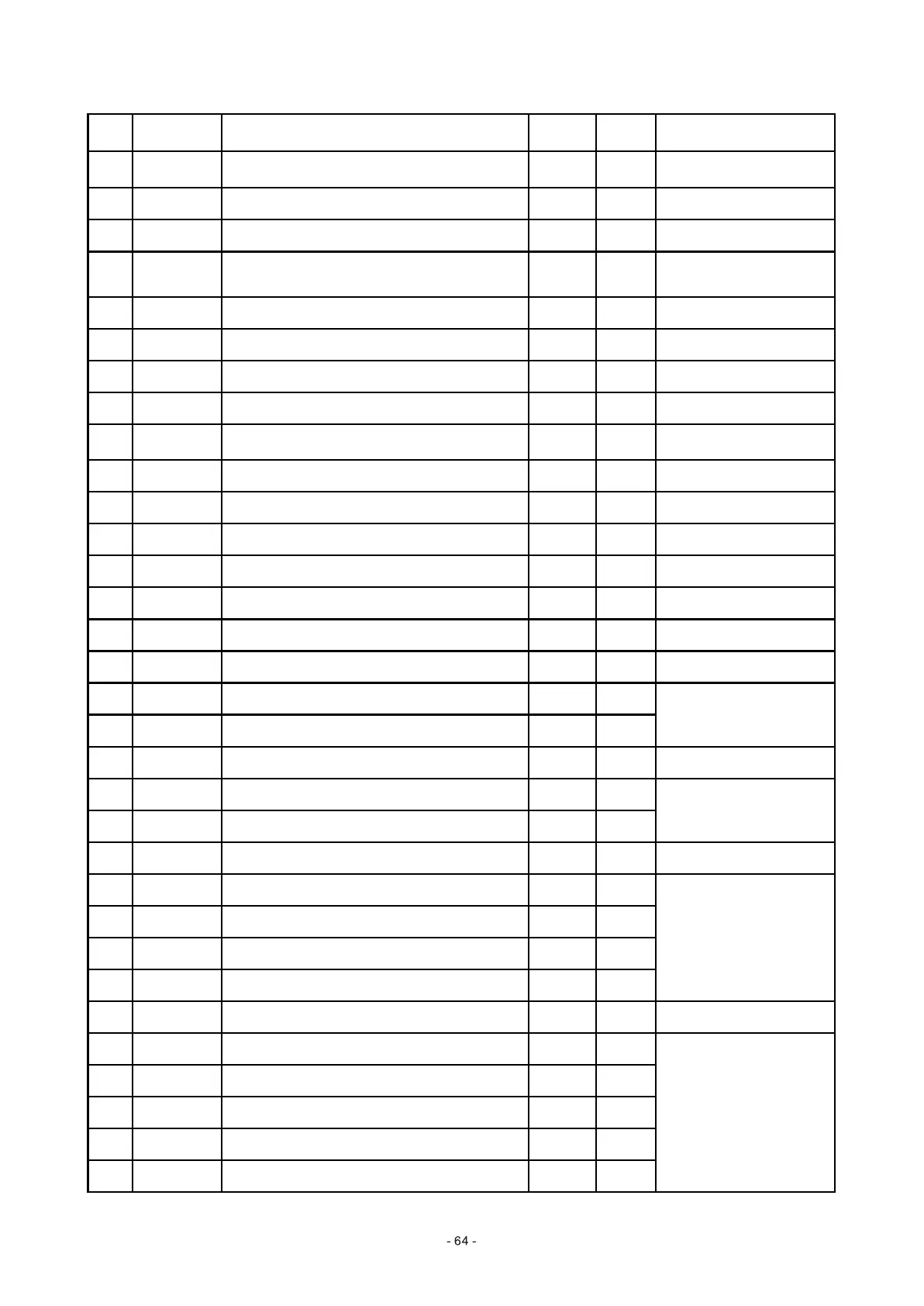
Pin Name Function
Data
direction
DC
voltage
Remark
101 UP1_5 Microcontroller port O 5.2
Panel communication-
enable
102 UP1_6 Microcontroller port O 0.3 I2C clock
103 UP1_7 Microcontroller port I/O 3.22 I2C data
104 UP3_0 Microcontroller port O 0
Tuning signal after being
managed from SAA6588
105 UP3_1 Microcontroller port O 0.68
106 UP3_4 Microcontroller port I/O 3.8 Serial communication port
107 UP3_5 Microcontroller port I/O 3.23 Serial communication port
108 DVDD3 Power supply 3.24
109 ICE Microcontroller correction mode enable 0
Ground through 1K resistor
R213
110 PRST Reset input I 3.3
111 IR Remote control signal input I 5.03
112 INT0 Microcontroller interrupt 0 I 3.6 unused
113 DQM0 DRAM input/output screen-shielded signal O 2.2
114 DQS0 DRAM input/output screen-shielded signal O 3.22
115 RD7 DRAM data I/O 0.9 SDRAM data line
116 DVSS Ground 0
117 RD6 DRAM data I/O 0.4
118 RD5 DRAM data I/O 0.85
119 DVSS Ground 0.02
120 RD4 DRAM data I/O 1.62
121 RD3 DRAM data I/O 1
122 DVDD18 Digital 1.8V power supply 1.9
123 RD2 DRAM data I/O 1.15
124 RD1 DRAM data I/O 0.92
125 RD0 DRAM data I/O 0.92
126 RD15 DRAM data I/O 0.66
127 DVDD3 Digital 3.3V power supply 3.21
128 RD14 DRAM data I/O 1.2
129 RD13 DRAM data I/O 1.2
130 RD12 DRAM data I/O 1.42
131 RD11 DRAM data I/O 0.85
132 RD10 DRAM data I/O 0.87
SDRAM data line
SDRAM data line
SDRAM data line
SDRAM data line