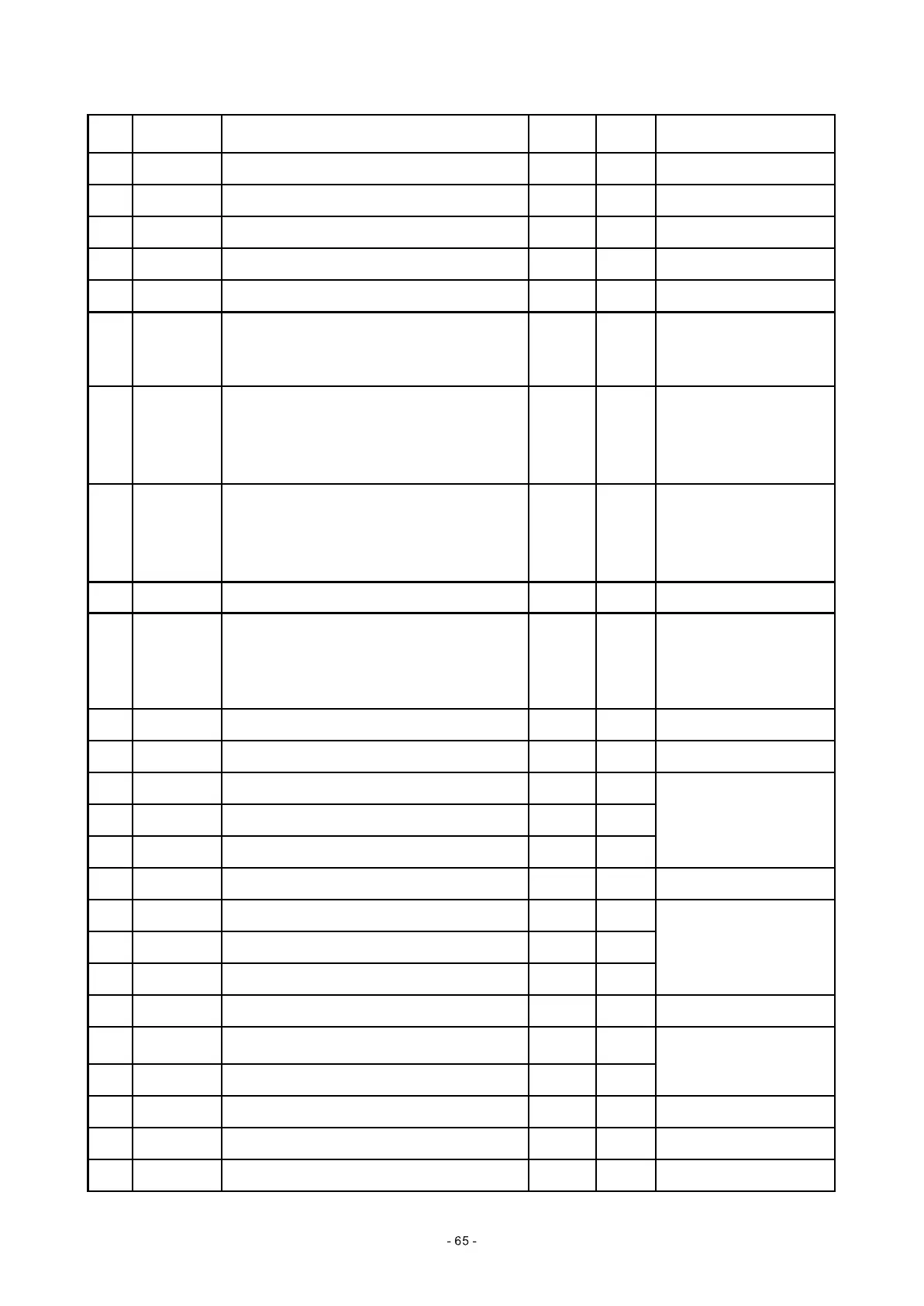
Pin Name Function
Data
direction
DC
voltage
Remark
133 RD9 DRAM data I/O 0.98 SDRAM data line
134 DVSS Ground 0.01
135 RD8 DRAM data I/O 0.67 SDRAM data line
136 DQS1 DRAM input/output screen-shielded signal O 3.24
137 DQM1 DRAM input/output screen-shielded signal O 2.6
138 RWE DRAM write enable O 3.17
Output WE# signal and
change into DWE# to
control the write of SDRAM
through 33 ohm resistor
139 CAS DRAM line address selection O 3.11
Output RAS# and change
into DCAS# to control line
address selection of
SDRAM through 33 ohm
resistor R267
140 RAS DRAM row address selection O 3.15
Output RAS# and change
into DRAS# to control row
address selection of
SDRAM through 33 ohm
resistor R266
141 DVDD3 Digital 3.3V power supply 3.22
142 RCS DRAM chip selection O 2.7
Output CS# and change
into DCS# to control chip
selection of SDRAM
through 33 ohm resistor
265
143 BA0 DRAM section address 0 O 1.75
144 DVSS Ground 0
145 BA1 DRAM section address 1 O 1.95
146 RA10 DRAM address O 0.04
147 RA0 DRAM address O 0.4
148 DVSS Ground 0
149 RA1 DRAM address O 2.2
150 RA2 DRAM address O 2.25
151 RA3 DRAM address O 1.57
152 DVDD18 Digital 1.8V power supply 1.91
153
RVREF/ADIN
3
Reference voltage/AD universal input I 0.01
154 RCLKB DRAM clock O 0.01
155 DVDD3 Digital 3.3V power supply 3.21
156 RCLK DRAM clock O 1.66
157 CKE DRAM clock enable O 1.2
SDRAM address line
SDRAM address line
unused