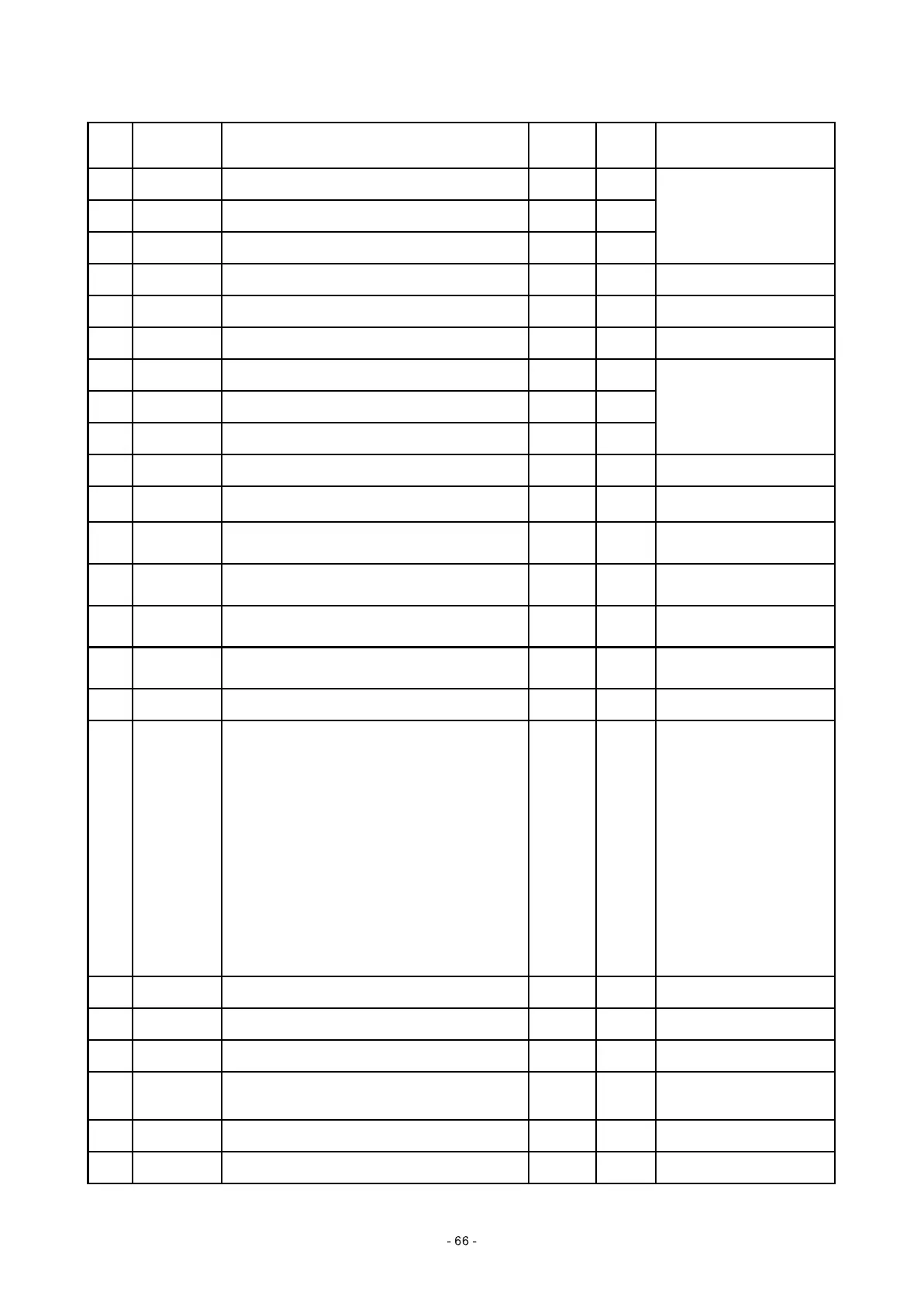
Pin Name Function
Data
direction
DC
voltage
Remark
158 RA11 DRAM address O 0.03
159 RA9 DRAM address O 0.07
160 RA8 DRAM address O 0.04
161 DVSS Digital 0
162 RA7 DRAM address O 1.4 SDRAM address line
163 DVSS Digital 0
164 RA6 DRAM address O 1.44
165 RA5 DRAM address O 1.74
166 RA4 DRAM address O 1.63
167 DVDD3 Digital 3.3V power supply O 3.21
168
RD13/ASDA
TA5
DRAM data/audio serial data I
5.04/3.0
3
Digital potentiometer input
(J3)
169 RD30 DRAM data I/O 0.01
Digital potentiometer inpout
(J4)
170 RD29 DRAM data O 0.01
CD4052 select signal
(AUNIN SL0)
171 RD28 DRAM data 0.01
CD4052 select signal
(AUNIN SL1)
172 RD27 DRAM data 0.01
select signal of N4
74HCT125
173 DVDD18 Digital 1.8V power supply 1.91
174 RD26 DRAM data I/O 3.6
Output to N12. When
headphone is not inserted,
output 3.3V, and now the
output to headphone from
N12 has no waveform.
When headphone is
inserted, this pin outputs
0v, and now only the output
to headphone and to
left/right channel of AV
board of N12 output have
waveform, which is
headphone select signal.
175 DVSS Digital I/O 0 Ground
176 RD25 DRAM data I/O 3.6 Mute signal
177 RD24 DRAM data I/O 1.68
178 DQM3 DRAM input/output screen-shielded signal O 0.04
Resistor R225 is unused,
so this signal is unused in
this model.
179 DQM2 DRAM input/output screen-shielded signal O 0.01 Field sync signal
180 RD23 DRAM data I/O 0.01 unused
SDRAM address line
SDRAM address line