1
Table of Contents
SAFETY INFORMATION...................................................................................................................................................... 2
ELECTROSTATIC DISCHARGE SENSITIVE (ESDS) DEVICE HANDLING ...................................................................... 3
SPECIFICATIONS ................................................................................................................................................................ 4
FREQUENCY CURVES........................................................................................................................................................ 6
Figure 1. 402 EQ Card HF Only Response ................................................................................................................... 6
Figure 2. 402 EQ Card Full Range Response ............................................................................................................... 6
Figure 3. 502A EQ Card HF Only Response ................................................................................................................. 7
Figure 4. 502A EQ Card Full Frequency Response ...................................................................................................... 7
Figure 5. 502B EQ Card Response ............................................................................................................................... 8
Figure 6. 802 EQ Card HF Only Response ................................................................................................................... 8
Figure 7. 802 EQ Card Full Range Response ............................................................................................................... 9
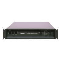
Figure 8. 1800-V Block Diagram.................................................................................................................................. 10
THEORY OF OPERATION ..................................................................................................................................................11
1. GENERAL........................................................................................................................................................................11
2. CIRCUIT DESCRIPTIONS.............................................................................................................................................. 12
3. PROTECTION CIRCUITRY ............................................................................................................................................ 17
1800-V DISASSEMBLY/ASSEMBLY PROCEDURES...................................................................................................... 20
Figure 9. Cover's Attaching Hardware ......................................................................................................................... 20
Figure 10. Rear View - Attaching Hardware................................................................................................................. 22
Figure 11. 240V Configuration ..................................................................................................................................... 22
Figure 12. 1800-V Amplifier Assembly ......................................................................................................................... 22
Figure 13. Bottom Mounted Components. ................................................................................................................... 25
Figure 14. Side View - Bottom Mounted Components................................................................................................. 25
Figure 15. Heatsink Bridge .......................................................................................................................................... 26
TEST PROCEDURES......................................................................................................................................................... 29
AMPLIFIER TEST PROCEDURES .................................................................................................................................... 29
EQ CARD TEST PROCEDURES ....................................................................................................................................... 30
PART LISTS AND EXPLODED VIEWS ............................................................................................................................. 33
1800-V MAIN ASSEMBLY PART LIST .............................................................................................................................. 34
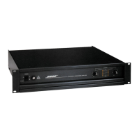
Figure 16. Front Panel Views....................................................................................................................................... 37
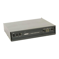
Figure 17. Back Panel View......................................................................................................................................... 37
Figure 18. Cross Section View..................................................................................................................................... 37
Figure 19. Top Down Inside Views............................................................................................................................... 38
1800-V PACKAGING PART LIST ...................................................................................................................................... 39
Figure 20. 1800-V Amplifier and EQ Card Packaging Illustration ................................................................................ 39
1800-V ELECTRICAL AND MECHANICAL PART LISTS ................................................................................................. 40
Display PCB Electrical Part List ................................................................................................................................... 40
I/O PCB Electrical Part List .......................................................................................................................................... 42
Power Supply PCB Electrical Part List ........................................................................................................................ 45
Regulator PCB Electrical Part List ............................................................................................................................... 49
Power Switch PCB Electrical Part List ......................................................................................................................... 51
Amplifier PCB Electrical Part List................................................................................................................................. 52
Output PCB Electrical Part List .................................................................................................................................... 55
Input Module PCB Electrical Part List .......................................................................................................................... 57
402 Equalizer PCB Assembly Electrical Part List ........................................................................................................ 60
502A Equalizer PCB Assembly Electrical Part List ...................................................................................................... 61
502B Equalizer PCB Assembly Electrical Part List ...................................................................................................... 63
802 Equalizer PCB Assembly Electrical Part List ........................................................................................................ 64
WIRING DIAGRAMS .......................................................................................................................................................... 66
Figure 21. 1800-V Wiring Diagram .............................................................................................................................. 66
Figure 22. 1800-V 240V Wiring Diagram Variation Difference..................................................................................... 67
SCHEMATICS AND PCB LAYOUTS ................................................................................................................................. 68
402 Equalizer Card Schematic .................................................................................................................................... 69
502A Equalizer Card Schematic .................................................................................................................................. 70
502B Equalizer Card Schematic .................................................................................................................................. 71
802 Equalizer Card Schematic .................................................................................................................................... 72
402, 502A AND 802 Equalizer Card PC Board Layout, P/N 177328, Revision 01 ................................................. 73
502B Equalizer Card PC Board Layout, P/N 178860, Revision 0 ........................................................................... 74
CAUTION: THE 1800-V PROFESSIONAL STEREO POWER
AMPLIFIER SYSTEM CONTAINS NO USER-SERVICEABLE PARTS.
TO PREVENT WARRANTY INFRACTIONS, REFER SERVICING TO
WARRANTY SERVICE STATIONS OR FACTORY SERVICE.