57
Power Supply (continued)
The center-”Off” power switch [Switch PCB, C3] selects immediate (ON) or sequenced
(STANDBY) amplifier power control. When set to “On”, current is applied through the switch
directly to the power transformer primary.
Set to “Standby”, the power switch routes current to triac Q100 [AC I/O, D2] and to “Standby”
LED D3 [Switch PCB, D4], lighting the LED. In standby mode, the amplifier is powered up by
application of a positive 7 to 15 VDC control voltage to the sequence “RCV” terminal (J801p3)
[Interface PCB, B4]. After a delay set by the RC network on its base, Q801 [F4] turns on and
relays the control voltage to the sequence “SND” terminal (J801p2) [B4]. The control voltage also
biases Q802 [G4] on, sourcing current from Q803 [G4] via P802p2 [H4] to J100p2 [AC I/O, C2] to
turn on the LED section of opto-isolator U100 [D2]. The output half of U100 supplies gate voltage
to fire triac Q100 [D2], supplying current to the transformer. Control current is drawn from the
“RCV” input terminal (J801p3) [Interface PCB, B4] until the amplifier 15V power supply turns on.
The sequence circuitry on the Interface Assy operates in parallel with the sequence circuitry on
the input module. The amplifier may be powered up using either RCV input, and both SND
outputs will supply control voltage to additional amplifiers. A ground terminal (J801p1) [B4] is
supplied at chassis-mounted sequence connector J801 for convenient connection of control
voltage common.
The power transformer secondary feeds two full-wave rectifier and filter circuits. The high volt-
age taps (red leads) feed bridge rectifier D402 [Power Supply PCB, C3] and filter capacitors
C404, C406 to supply ±43 VDC (loaded) VS
POS
and VS
NEG
rails to the power amplifier stage via
P600 [F2]. Fuses F400, F401 [D3] limit power dissipation under amplifier fault conditions. The
low voltage taps (yellow leads) feed bridge rectifier D400/ D401/ D404/ D405 [C4] and filter caps
C405, C407, providing raw power to linear regulators U400, U401 [E4/5], U402 and U403 [F4/5]
for the ±15V analog processing and control circuit power supplies. Fuses F402, F403 [D4]
provide fault protection. Three +15 V and two –15 V regulated supply rails are generated. This
enhances isolation between functional blocks and spreads the supply current demand across
multiple devices. The amplifier star ground [E3] is connected to the chassis via a Rectifier Assy
mounting standoff.
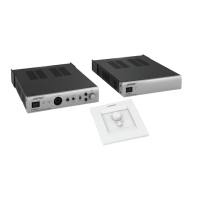
Input Module
Note: Some amplifiers will be equipped with the Bose
®
ACM-1 Amplifier Control Module in place
of the standard Bose Input Module. This module retains all of the capabilities of the Bose Input
Module, except sequence, and includes the ability to control and monitor the amplifier over a
control network. Refer to the ACM-1 Amplifier Control Module service manual, part number
199746 for more information.
Note: Refer to the Input Module PCB schematic sheets for the following information. The desig-
nations inside the brackets “[ ]” indicate the grid coordinates for the component described.
The Input Module consists of signal input connections, mode switching, optional equalization,
and power sequencing circuitry. The module operates from +15V and -15V, supplied by the host
amplifier through J2-2 and J2-1 [sheet1, H4] respectively.
THEORY OF OPERATION