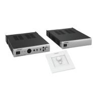
59
Input Module (continued)
In DUAL MONO mode both amplifier channels are driven by the signal applied to the CH2 input.
U6-1 is driven high (+15V) and U5-1 is driven low (+7.5V), selecting CH2 to drive both channels
of the amplifier.
In BRIDGED MONO operation the CH2 signal is routed directly from the equalizer switch U3 to
the amplifier inputs. U5 control pin 1 is driven low (+7.5V) selecting the inverting input of the op-
amp switching IC signal. This inverting signal is then sent to the B input of U6 whose control
signal at pin 1 is driven low selecting the B input. This routes the inverted signal to the CH1 input
of the amplifier.
Signal Processing
Note: Refer to the Signal Processor PCB schematic sheets for the following information. The
designations inside the brackets “[ ]” indicate the grid coordinates for the component described.
Signal from the input module via input cable P100 [sheet1, A3] is supplied to U501B [B1], which
drives CH1 Effects Send hot output J804p1 [Interface PCB, B3]. U501A [sheet 1, B2] provides a
clean, isolated signal ground reference for CH1 Effects Send common output J804p2 [Interface
PCB, B3]. Effects Receive input (J804p3&4) is applied to differential amplifier U500A [Signal
Processor sheet1, B2], which rejects common-mode noise and produces signal ground refer-
enced output.
Use of switched output op-amps provides convenient signal routing via remotely set control
voltages. Switched op-amp U503 [D2] selects amplifier input source. Signal from the input
module is applied to U503 section A, while signal from the CH1 Effects Receive input is applied
to U503 section B. Control input U503p1 routes U503 section A signal to output U503p5 when
pulled up to +15V through R521, but routes U503 section B signal to output U503p5 when
grounded through R517 by configuration DIP switch S801E [Interface PCB, B5].
Input U505p3 monitors CH1 signal level, driving circuitry that lights the “Signal” LED when input
level exceeds –36dBu. U505A [Signal Processor sheet1, D1] provides 40dB of AC gain, with
D509 limiting peak positive output to 7.5V and negative output to -0.6V. Output U505p1 drives
rectifier D510 and filter C544 through current limiting resistor R542. Filtered voltage is applied to
Q501 [E1] base via R550, R552 network, biasing Q501 on when C544 voltage exceeds 1.4V.
Q501 sinks current through limiting resistor R556 lighting “Signal” LED D709 [Display PCB, D2]
(J700p16 Signal Processor Assy to P700p16 Display Assy).
A voltage controlled amplifier circuit provides amplifier signal level control and voltage gain. VCA
U511 [Signal Processor sheet1, D2] is a current input, current output device whose gain is set by
control voltage applied to U511p3. VCA input U511p1 is a virtual ground, with input current
determined by the ratio of input voltage to R569 resistance. VCA output current from U511p8
drives transimpedance amplifier U512A to produce output voltage at U512p1 equal to the product
of output current and R568 resistance. Voltage gain of the level control block is Vout/Vin =
k*(R568/R569) = k*3.65, where k is VCA gain. R6 and trimpot R1 allow manual bias adjustment
to minimize VCA distortion.
THEORY OF OPERATION