61
Signal Processing (continued)
Limiter operation can be disabled through the ACM-1 control interface by pulling J101p17 [Signal
Processor sheet2, B5] to ground. Q427 [E3] also turns on when clip detector output U427p2 is
pulled up, sinking current through limiting resistor R441 lighting “Clip” LED D715 [Display PCB,
D3] (J700p14 Signal Processor Assy to P700p14 Display Assy).
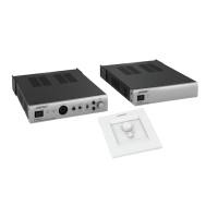
Power Amplifier PCB
The M2150 employs digital power amplifier technology to achieve high efficiency with high fidelity.
Note: This section describes the operation of the original version of the amplifier and driver
module PCB assemblies, board part number 6000.0435 only.
Refer to the Power Amplifier PCB schematic sheet for the following information. The designa-
tions inside the brackets “[ ]” indicate the grid coordinates for the component described.
Signal input (header J601p9 Signal Processor Assy via cable J601p9 Power Amp Assy) [Power
Amplifier PCB, A3] is applied to input resistor R602 [B3] and coupled through C614 to digital
amplifier driver input U605p6 [D/E3]. The combined series resistance of R576 [Signal Processor
sheet1, G2] and R602 sets power amplifier gain to 5.35. Digital amplifier driver U605 processes
the audio signal input to generate a spread-spectrum modulation pattern that varies in frequency
from approximately 200kHz to 1.5MHz. Complementary copies of this modulation pattern are
level-shifted by internal gate drivers and used to control external N-channel MOSFETs Q610
[Amplifier PCB, F4], Q611 [F5] connected in half-bridge configuration. Gate resistors R624, R625
set MOSFET switching speed, diodes D610, D611 clamp reverse voltages across the
MOSFETs, C635, C636 and C653 provide local HF bypassing. The half-bridge output is a power-
amplified version of the modulation pattern that switches between VS
POS
and VS
NEG
. Lowpass
filter L610, C658 [G5] integrates the switched output waveform to yield demodulated, amplified
audio. Zobel network R642, C661 provides a constant HF load for the output filter to damp filter
resonance under lightly loaded conditions. Power amplifier output is connected to output hot
terminal WL610 [H5] through current sense resistor R646: voltage across R646 is fed through
R643, R650 to the ACM-1 control interface (cable J601p1&2 [A3] Power Amp Assy to header
J601p1&2 Signal Processor Assy to J101p3&4 [Signal Processor PCB sheet2, B5]).
Driver control feedback is taken from the half-bridge output directly at the LC filter input through
delay network R640, C656 [Amplifier PCB, F4] to U605p18. Ground voltage at output common
terminal WL611 is monitored and corrected via kelvin ground sense input U605p9.
To minimize output stage shoot-through currents, the digital amplifier driver inserts dead time
between turnoff of one MOSFET and turn on of the other. Break before make delay of 25, 60, 105
or 145ns is selected by tying control bits BBM0, BBM1 (U605p7,8) to 5V or ground as desired.
The default setting is 25ns, chosen for best THD performance.
The power amplifier includes a servo circuit that minimizes output DC offset; desirable since the
amplifier output is transformer coupled. Amplifier output voltage is sampled at the LC filter output
by integrator U603B [C6]. U603A [C6] inverts integrator output to restore sign and adds a 2.5V
offset to pre-range the output signal, which is further low pass filtered by R605 and C616 [C3].
The error voltage drives correction current into driver input U605p6 through R604. Note that the
digital amplifier driver is inverting: input and output are out of phase. Should amplifier DC offset
rise, servo circuit output will rise, feeding current into the driver input and forcing the output back
to ground.
THEORY OF OPERATION