■ BCM5221 Product Application Note
■ BCM5220 7/7/00
Broadcom Corporation
Page 13 5221/5220-AN01 Product Application Note, Revision R
JTAG FUNCTIONAL DESCRIPTION
The JTAG_EN signal should be set to a high logic level to enable JTAG function since JTAG signals are multiplexed with
other signals during normal operation. Once enabled, TCK, TRST#, TMS, TDI and TDO provide JTAG functionality. Please
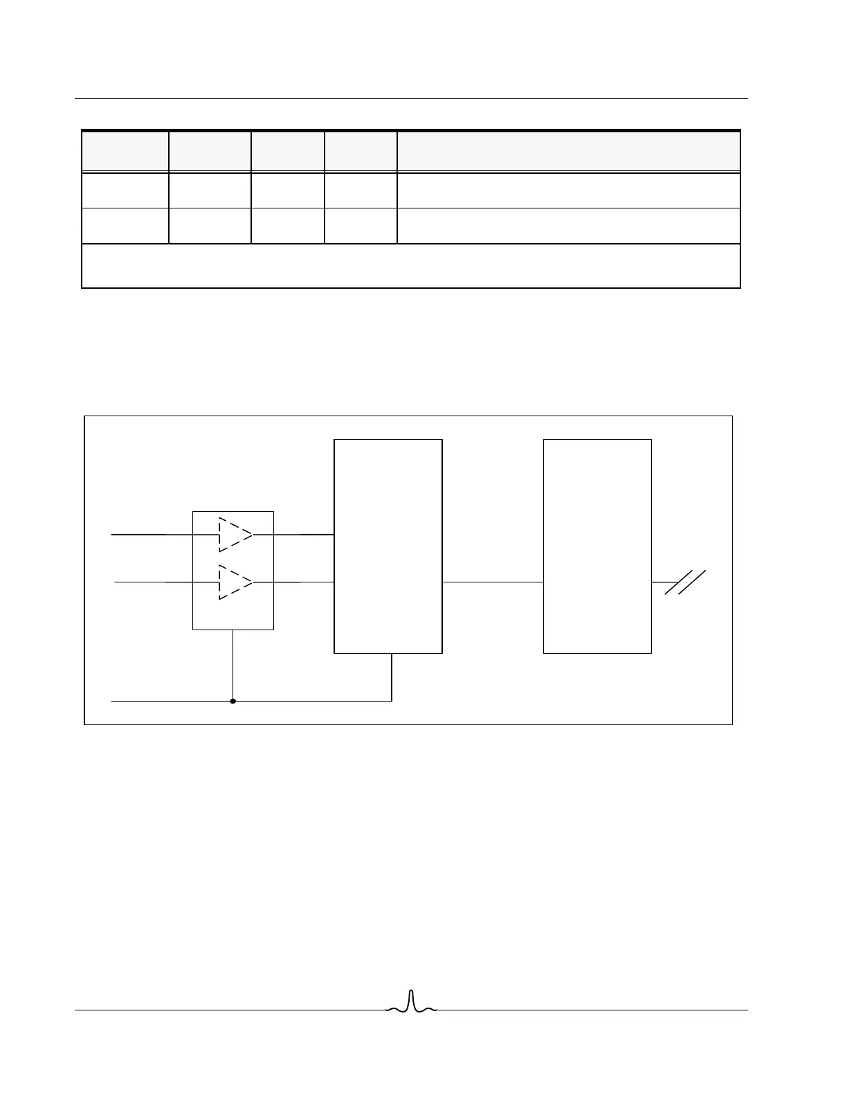
refer to the following schematics to connect JTAG signals and JTAG compatible devices to JTAG chain.
Figure 7: JTAG Chain Schematics
Setting JTAG_EN to a high level causes the BCM5221 to enter JTAG mode. You must connect the JTAG TDI and TMS input
signals to the BCM5221 TDI and TMS input signals through tri-state buffers as shown in the above schematics because
these inputs are multiplexed with other output signals during normal operation.
ELIMINATING TRI-STATE BUFFER REQUIREMENT
Preferred Method. If the design does not require LNKLED# and SPD_LED# signals, it is possible to connect the JTAG
TDI and TMS signals directly to the TDI and TMS pins of the BCM5221. Eliminating the TDI tri-state buffers is accomplished
by the following two writes.
1 Enable shadow register by writing a 1to bit 7 of MII register 1Fh.
2 Write a 1 to bit 3 of MII shadow register 1Ah.
TDI I/O
PU
H8 35 Test Data Input. This signal is multiplexed with LNKLED# and
MEDIA_CONV# signals.
TDO I/O
PU
H7 33 Test Data Output. This signal is multiplexed with RCVLED#,
ACTLED# and MDIX_DIS signals.
I
PD
= Input with internal pull-down. I
PU
= Input with internal pull-up.
I/O
PD
= Input/Output with internal pull-down. I/O
PU
= Input/Output with internal pull-up.
Table 2: JTAG Signals (Cont.)
JTAG Signal Type
BCM5221
KPB
BCM5221
KPT
Description
Enable JTAG
TDI
JTAG_EN
TDI TDO
TCK
TRST#
TMS
BCM5221
TRISTATE
BUFFER
EN
TMS
TDI TDO
TCK
TRST#
TMS
JTAG
DEVICE