■ BCM5221 Product Application Note
■ BCM5220 7/7/00
Broadcom Corporation
Page 3 5221/5220-AN01 Product Application Note, Revision R
• TESTEN > pull-down
• LOWPWR > pull-down
• MDIO > pull-up
• RESET# > pull-up
• F100 > pull-up
• ANEN > pull-up
• MII_EN > Pull-up
• LNKLED# > pull-up
• SPDLED# > pull-up
• RCVLED# > pull-up
The XMTLED#/INTR#/FDXLED# output is Open Drain
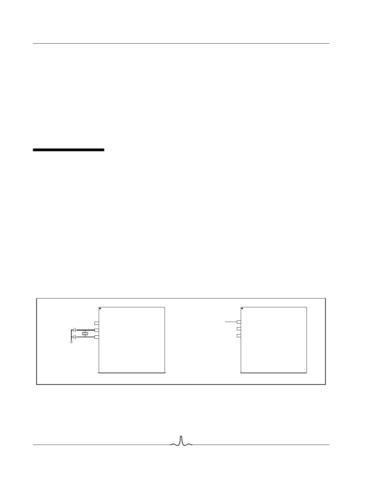
25 MHZ REFERENCE CLOCK
The BCM5221 device accepts a 25 MHz (or 50MHz for RMII applications) reference clock from either a low cost crystal circuit
(parallel resonance operating in the fundamental mode) or a single ended clock source such as a 50 ppm self-contained
oscillator or buffered system clock. See Figure 2 for clock connection requirements.
For stand-alone crystal applications, Broadcom recommends that the crystal is located as close to the XTALI and XTALO
pins of the BCM5221 as possible to minimize stray capacitance due to excessive trace routing that could interfere with crystal
start-up as well as clock stability.
Broadcom recommends the use of a crystal rated for a total load capacitance of 18 pF. A calculation for deriving the approx-
imate load capacitance is: ((C
L1
xC
L2
)/(C
L1
+C
L2
)) + C
s
Where C
L1
xC
L2
are the actual load capacitors connected to either
side of the crystal, and C
s
is the sum of the stray capacitance and input pin capacitance of the PHY device. Assuming load
caps of 20pF each and a total stray + parasitic capacitance of approximately 8pF, the above equation yields a total load
capacitance of around 18pF. The load capacitor values may need to be adjusted from the example above to account for
variations in parasitic capacitance and/or crystal specification.
For applications using an XTAL based oscillator or buffered system clock, the REF_CLK input should be used. In this in-
stance, the XTALI input should be pulled to ground (4.7K) and the XTALO pin can remain unconnected. The input voltage
swing of the reference clock must be no greater than the voltage at the OVDD power pin.
Figure 2: Oscillator Clock Considerations
The electrical specifications recommended for the crystal or oscillator clock source are as follows:
• Frequency tolerance: +/-50 ppm
• 50% Duty Cycle: +/- 10%
BCM5221
(XTAL Connection)
BCM5221
(Reference Clock)
+/-50ppm
18pF
18pF
25MHz (MII)
XTALI
XTALO
XTALI
XTALO
REF_CLKN/C
REF_CLK