User’s Manual
13
CN7: Pin Header for PS2 KB / MS
Pin No. Signal (KB) Pin No. Signal(MS)
1 KB Data 2 MS Data
3 KEY 4 KEY
5 GND 6 GND
7 +5V(DC) 8 +5V(DC)
9 KB_CLK 10 MS_CLK
Printer (LPT1/LPT2) Port
Pin No. Description Pin No. Description
1 STB# 10 ACK#
2 PD0 11 BUSY
3 PD1 12 PE
4 PD2 13 SLCT
5 PD3 14 AFD#
6 PD4 15 ERR#
7 PD5 16 INIT#
8 PD6 17 SLIN#
9 PD7 18-25 GND
JP5: Voltage Selector for LDVS Receiver
Pin No. Signal
1-2 Receiver = +5V(DC) Type
2-3 Receiver = +3.3V(DC) Type
Open for OEM. Type 4-5
Close for Normal Type
* Caution: Improper setting will damage LCD panel.
CN5: LCD - LVDS Output.
Pin No. Signal Pin No. Signal
1 Y0– 2 Y2–
3 Y0+ 4 Y2+
5 Y1– 6 Rcv. Voltage
7 GND 8 Y3–
9 Y1+ 10 Y3
11 CK– 12 VDD_PNL
13 CK+ 14 DISP_OFF
15 VBL 16 GND
14
The ENDAT-3201M/MF/MH
Embedded CPU Board
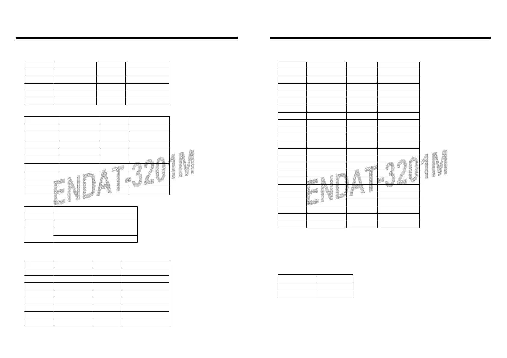
LCD_CON1: TFT LCD Panel Port
Pin No. Signal Pin No. Signal
1 VBL 2 VBL
3 GND 4 GND
5 VDDLCD 6 VDDLCD
7 ENPVEE 8 GND
9 FPD 23 10 FPD 22
11 FPD 17 12 FPD 16
13 FPD 11 14 FPD 10
15 FPD 9 16 FPD 8
17 FPD 21 18 FPD 20
19 FPD 15 20 FPD 14
21 FPD 7 22 FPD 6
23 FPD 5 24 FPD 4
25 FPD 19 26 FPD 18
27 FPD 13 28 FPD 12
29 FPD 3 30 FPD 2
31 FPD 1 32 FPD 0
33 GND 34 GND
35 P_CLK 36 FLM
37 DE 38 LP
39 GND 40 VDDLCD
41 VDDLCD 42
KEY
43 VDDLCD 44 VDDLCD
* Please make sure the Pin 1 location before inserting the LCD connector.
Please double-check the insertion and orientation of the LCD cable before applying power.
Improper installation will result in permanent damage LCD panel.
Factory Setting:
JP1: All Pin Open
JP7: LCD Voltage selector
Voltage JP7
3.3V 4-6
5V 2-4
JP8: Close Pin 1-2
JP13: Factory Using only
JP14: Close Pin 2-3; Pin 5-6; Pin 8-9; Pin 11-12
JT1: Close Pin 2-3; Pin 4-5; Pin 8-9
JH1: Close Pin 1-2; Pin 5-6; Pin 7-8