User’s Manual
29
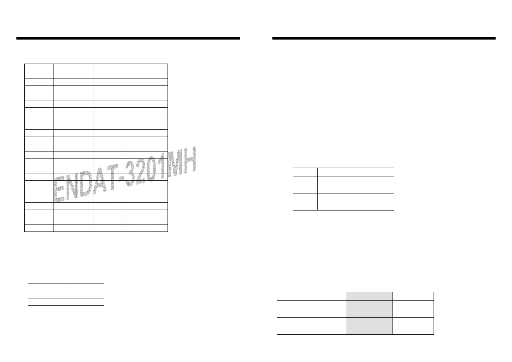
LCD_CON1: TFT LCD Panel Port
Pin No. Signal Pin No. Signal
1 VBL 2 VBL
3 GND 4 GND
5 VDDLCD 6 VDDLCD
7 ENPVEE 8 GND
9 FPD 23 10 FPD 22
11 FPD 17 12 FPD 16
13 FPD 11 14 FPD 10
15 FPD 9 16 FPD 8
17 FPD 21 18 FPD 20
19 FPD 15 20 FPD 14
21 FPD 7 22 FPD 6
23 FPD 5 24 FPD 4
25 FPD 19 26 FPD 18
27 FPD 13 28 FPD 12
29 FPD 3 30 FPD 2
31 FPD 1 32 FPD 0
33 GND 34 GND
35 P_CLK 36 FLM
37 DE 38 LP
39 GND 40 VDDLCD
41 VDDLCD 42
KEY
43 VDDLCD 44 VDDLCD
* Please make sure the Pin 1 location before inserting the LCD connector.
Please double-check the insertion and orientation of the LCD cable before applying
power. Improper installation will result in permanent damage LCD panel.
Factory Setting:
JP1: All Pin Open
JP13: Factory Using only
JP7: LCD Voltage selector
Voltage JP7
3.3V 4-6
5V 2-4
JT1: Close Pin 2-3; Pin 4-5; Pin 8-9
JH1: Close Pin 1-2; Pin 5-6; Pin 7-8
JP8: Close Pin 1-2
JP14: Close Pin 2-3; Pin 5-6; Pin 8-9; Pin 11-12
30
The ENDAT-3201M/MF/MH
Embedded CPU Board
2-4. Installing Memory
The ENDAT-3201M/MF/MH CPU board offers one 168pin DIMM sockets supporting up to
512MB of memory. The DIMM memory can be 100MHz (PC-100) or 133 MHz (PC-133).
2-5. Shared VGA Memory
The ENDAT-3201M/MF/MH is using built-in AGP VGA controller with share memory
architecture (SMA) -
AGP mode with 2MB to 8MB
of system memory. The amount of
video memory on motherboard determines the number of colors and the video graphic
resolution.
2-6. Installing Riser Card
Installing Riser Card (Max. 3 PCI Slot on Riser Card)
PCI Slot INT ADSEL
PCI 1 A,B,C,D AD24(Onboard LAN)
PCI 2 B,C,D,A AD23
PCI 3 C,D,A,B AD22
PCI 4 D,A,B,C AD21
There are two different riser cards that can be fitted to ENDAT-3201M/MF/MH CPU board.
The first one is a 98pin ISA only Bus riser card (traditional ISA Bus riser card), the second
one is a 188pins PCI/ISA riser card.
Please note: PCI/ISA riser cards jumper settings have to be matched with the
motherboard INT/AD-select jumper.
The default INT/AD-select for ENDAT-3201M/MF/MH All-In-One motherboard is listed in
the above table. However, it could be revised by changing
JP14 setting
for different
INT/AD-select. The following table shows the variable configurations:
INT/AD Configurations:
Expansion for PCI Slot * Close 1-2 Close 2-3
Expansion PCI 1 INT =A,B,C,D INT = B,C,D,A
Expansion PCI 2 INT = B,C,D,A INT = C,D,A,B
Expansion PCI 3 INT = C,D,A,B INT = D,A,B,C
Expansion PCI 4 INT = D,A,B,C INT = A,B,C,D
 Loading...