User’s Manual
27
J1: IR Pin Header.
Pin No. Function
1 +5V(DC)
2 N.C.
3 IRRX
4 GND.
5 IRTX
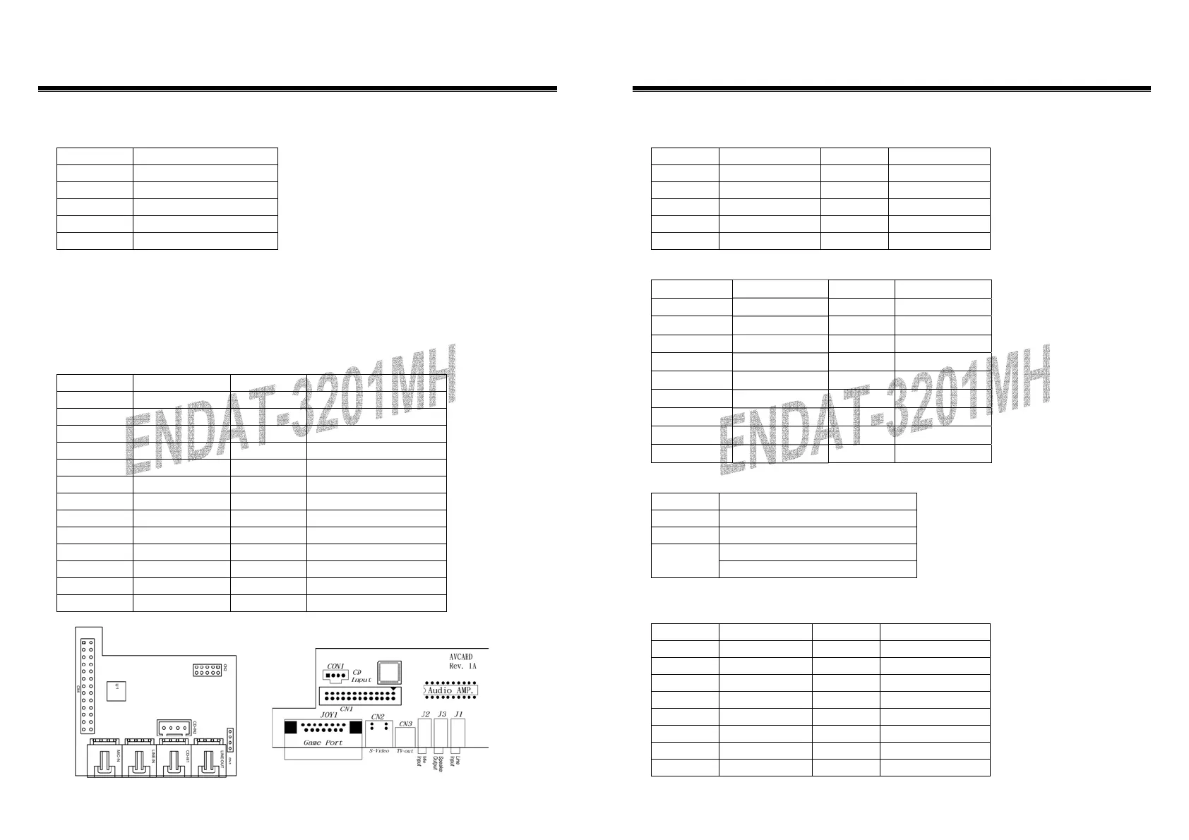
CN1: Audio Output Port connector via AV Card Kit (Optional)
Please close pin13-14 to disable onboard Audio features if the AV Card Kit is not
inserted onto the CN1 connector. If AV card kit is inserted, please make sure the
BIOS is enabled with the audio function, since LPT2 and audio function can not be
used in the same time.
CN1: Audio Port.
Pin No. Function Pin No. Function
1 BITCLK 2 GND
3 SDIN 4 N.C.
5 SDIN2 6 N.C.
7 SDOUT 8 N.C.
9 SYNC 10 GND
11 –ACRST 12 GND
13 SPEAK 14 Strapping Low
15 +5V(DC) 16 +12V(DC)
17 JBCY 18 JAB2
19 JBCX 20 JAB1
21 JACY 22 JBB2
23 JACX 24 JBB1
25 MSO 26 MSI
UC-A003
AV Card
28
The ENDAT-3201M/MF/MH
Embedded CPU Board
CN7: Pin Header for PS2 KB / MS
Pin No. Signal (KB) Pin No. Signal(MS)
1 KB Data 2 MS Data
3 KEY 4 KEY
5 GND 6 GND
7 +5V(DC) 8 +5V(DC)
9 KB_CLK 10 MS_CLK
Printer (LPT1/LPT2) Port
Pin No. Description Pin No. Description
1 STB# 10 ACK#
2 PD0 11 BUSY
3 PD1 12 PE
4 PD2 13 SLCT
5 PD3 14 AFD#
6 PD4 15 ERR#
7 PD5 16 INIT#
8 PD6 17 SLIN#
9 PD7 18-25 GND
JP5: Voltage Selector for LDVS Receiver
Pin No. Signal
1-2 Receiver = +5V(DC) Type
2-3 Receiver = +3.3V(DC) Type
Open for OEM. Type 4-5
Close for Normal Type
* Caution: Improper setting will damage LCD panel.
CN5: LCD - LVDS Output.
Pin No. Signal Pin No. Signal
1 Y0– 2 Y2–
3 Y0+ 4 Y2+
5 Y1– 6 Rcv. Voltage
7 GND 8 Y3–
9 Y1+ 10 Y3
11 CK– 12 VDD_PNL
13 CK+ 14 DISP_OFF
15 VBL 16 GND
 Loading...