EasyManua.ls Logo

Canon GP215 - III. Image Processing

Canon GP215
458 pages
Print Icon
To Next Page IconTo Next Page
To Previous Page IconTo Previous Page
Loading...
III. IMAGE PROCESSING
A. Outline
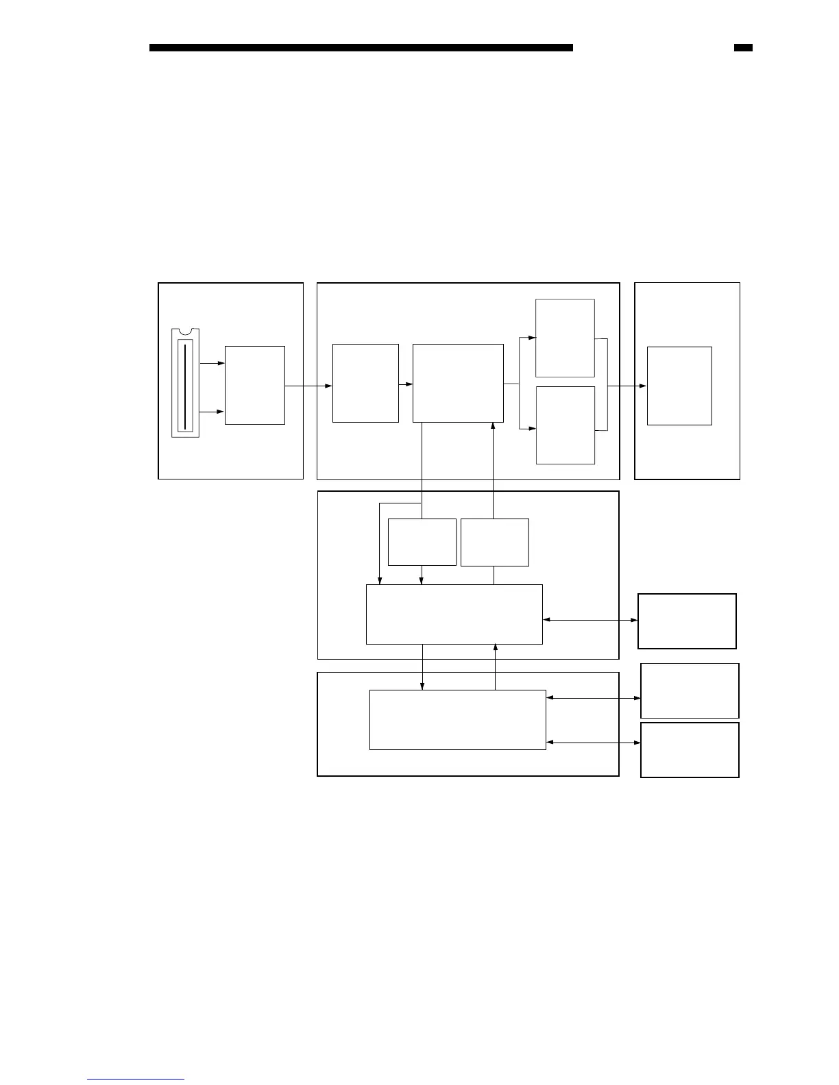
The image processing system converts the optical image projected on the CCD into electrical signals
(image signals) for correction and processing.
The correction/processing functions are by the following PCBs, and the results of correction/process-
ing are forwarded to the PCBs that follow them:
Figure 3-301
Analog processor
PCB
Image processor PCB
Laser driver
PCB
CCD
A-D
conversion
circuit
Shading
correction
circuit
Image
processing
circuit
Laser
driver
circuit
G3 FAX
Board/NCU
D/A
conversion
Binary
processing
Binary
processing
for fax
Reproduction
ratio
processing
CORE/IP
Board
Video signal
switching circuit
Command conversion
circuit
Protocol controller PCB
Printer
Board
Network I/F
Board
3–29
COPYRIGHT © 1996 CANON INC. CANON GP215/200 REV.0 JULY 1996 PRINTED IN JAPAN (IMPRIME AU JAPON)
3. OPERATIONS AND TIMING

Table of Contents