3. System Clock
3.1 General
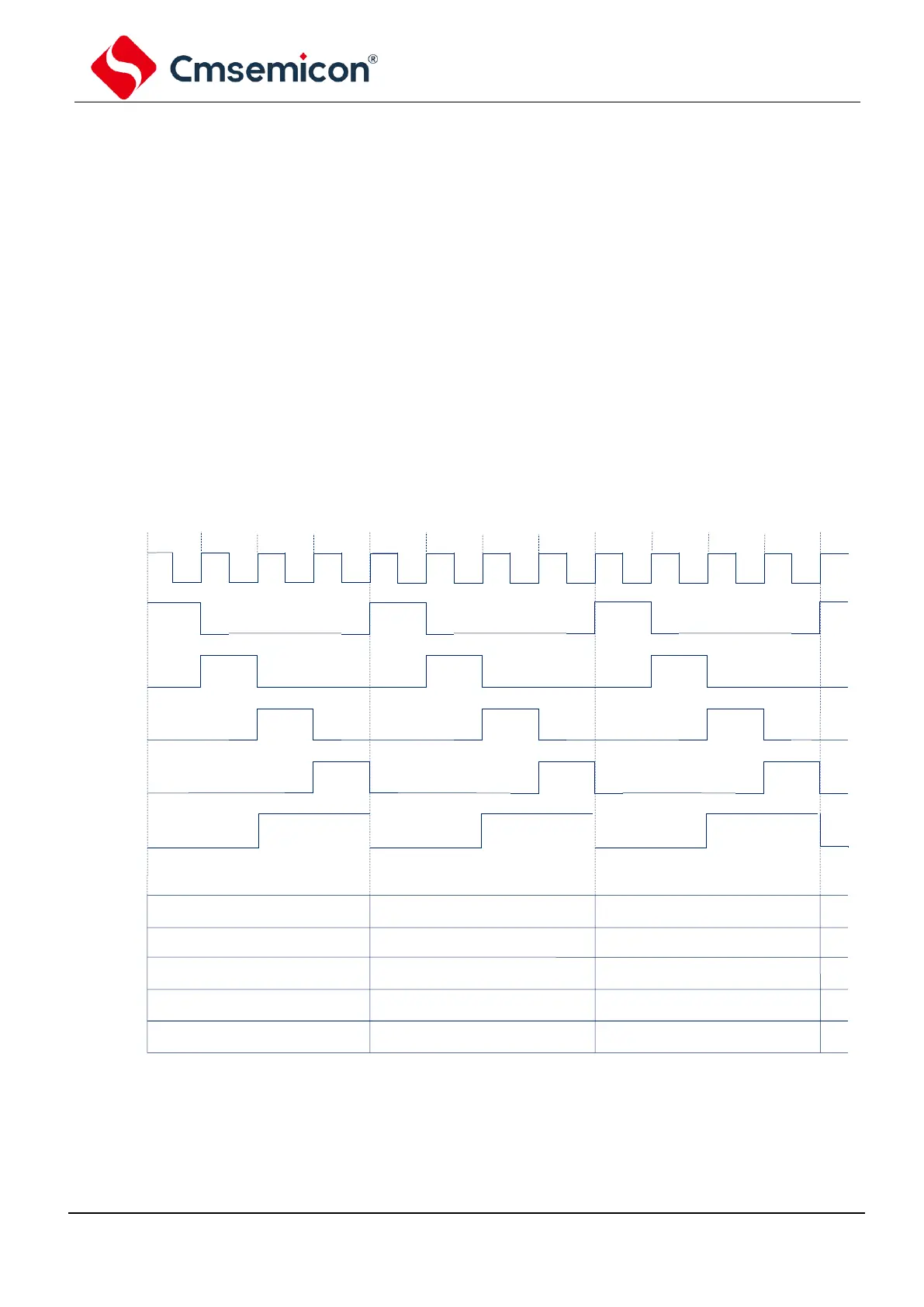
When clock signals input from OSCIN pin (or generated by internal oscillation), 4 non-overlapping
orthogonal clock signals called Q1、Q2、Q3、Q4 are produced. Inside IC , each Q1 makes program counter
(PC)increase 1, Q4 obtain this instruction from program memory unit and lock it inside instructions register.
Compile and execute the instruction obtained between next Q1 and Q4, which means that 4 clock period for
1 executed instruction. The following diagram illustrate the time series of clock and execution of instruction
period.
1 instruction period contains 4 Q period. The execution of instructions has pipeline structure. Obtaining
instructions only require 1 instruction period, compiling and executing use another instruction period. Since
pipeline structure is used, the effective executing time for every instruction is 1 instruction period. If 1
instruction cause PC address to change (such as JP), then the pre-loaded instruction code is useless and 2
instruction period is needed to complete this instruction. This is why every operation on PC consumes 2 clock
period.
Fig 3-1:time series for clock and instruction period


 To Next Page