EasyManua.ls Logo

Cmsemicon SC8F577 Series - Page 84

Default Icon
181 pages
Print Icon
To Next Page IconTo Next Page
To Previous Page IconTo Previous Page
Loading...
V1.8
SC8F577x
84 / 181
www.mcu.com.cn
PWM control register PWMCON1 (14H)
14H
Bit7
Bit6
Bit5
Bit4
Bit3
Bit2
Bit1
Bit0
PWMCON1
PWMIO_SEL[1:0]
PWM2DTEN
PWM0DTEN
---
---
DT_DIV[1:0]
R/W
R/W
R/W
R/W
R/W
---
---
R/W
R/W
Reset value
0
0
0
0
---
---
0
0
PWM control register PWMCON2 (1DH)
1DH
Bit7
Bit6
Bit5
Bit4
Bit3
Bit2
Bit1
Bit0
PWMCON2
---
---
---
PWM4DIR
PWM3DIR
PWM2DIR
PWM1DIR
PWM0DIR
R/W
---
---
---
R/W
R/W
R/W
R/W
R/W
Reset value
---
---
---
0
0
0
0
0
PWM0~PWM3 lower bit of period register PWMTL (15H)
15H
Bit7
Bit6
Bit5
Bit4
Bit3
Bit2
Bit1
Bit0
PWMTL
PWMT[7:0]
R/W
R/W
R/W
R/W
R/W
R/W
R/W
R/W
R/W
Reset value
0
0
0
0
0
0
0
0
Bit7~6
PWMIO_SEL[1:0]:
PWM IO selection
11=
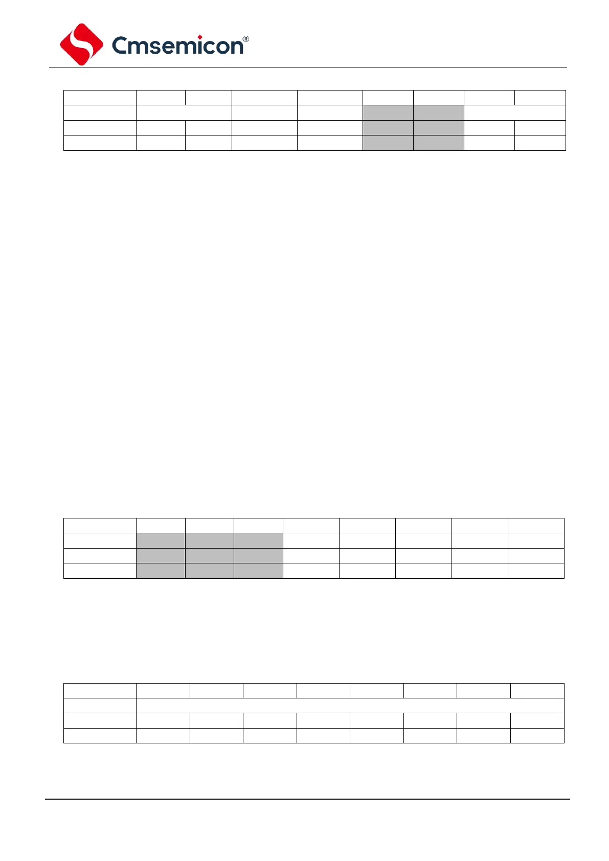
PWM assigned to group A, PWM0-RA0, PWM1-RA1, PWM2-RA2, PWM3-RA3, PWM4-
RA4
10=
PWM assigned to group B, PWM0-RA0, PWM1-RA1, PWM2-RA2, PWM3-RB2, PWM4-
RB1
01=
PWM assigned to group C, PWM0-RA5, PWM1-RA6, PWM2-RB6, PWM3-RB5, PWM4-
RB4
00=
PWM assigned to group D, PWM0-RB0, PWM1-RB1, PWM2-RB3, PWM3-RB4, PWM4-
RB2
Bit5
PWM2DTEN:
PWM2 dead-time enable bit
1=
Enable PWM2 dead-time function, PWM2 and PWM3 compose one pair of
complementary outputs.
0=
Disable PWM2 dead-time function.
Bit4
PWM0DTEN:
PWM0 dead-time enable bit
1=
Enable PWM0 dead-time function, PWM0 and PWM1 compose one pair of
complementary outputs.
0=
Disable PWM0 dead-time function.
Bit3
Not used.
Bit5
DT_DIV[1:0]:
Dead-time source clock division
11=
Fosc/8
10=
Fosc/4
01=
Fosc/2
00=
Fosc/1
Bit7~Bit5
Not used.
Bit4~Bit0
PWMxDIR:
PWMx output inversion control bit
1=
PWMx output inversion
0=
PWMx output ordinary
Bit7~Bit0
PWMT[7:0]:
Lower 8 bits of PWM0~PWM3 period register

Related product manuals